• Chinese Physics B
  • Vol. 29, Issue 8, (2020)
Ying Zan, Yong-Liang Li, Xiao-Hong Cheng, Zhi-Qian Zhao, Hao-Yan Liu, Zhen-Hua Hu, An-Yan Du, and Wen-Wu Wang
Author Affiliations
  • Integrated Circuit Advanced Process Center, Institute of Microelectronics, Chinese Academy of Sciences, Beijing 100029, China
  • show less
    DOI: 10.1088/1674-1056/ab973e Cite this Article
    Ying Zan, Yong-Liang Li, Xiao-Hong Cheng, Zhi-Qian Zhao, Hao-Yan Liu, Zhen-Hua Hu, An-Yan Du, Wen-Wu Wang. High crystalline quality of SiGe fin fabrication with Si-rich composition area using replacement fin processing[J]. Chinese Physics B, 2020, 29(8): Copy Citation Text show less
    SEM images of (a) Si fin profile, (b) Si fin exposure, (c) Si fin recess, and (d) SiGe’s selective epitaxial growth.
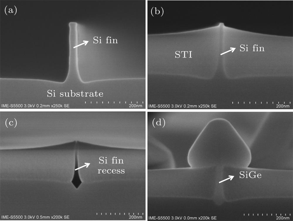
    Fig. 1. SEM images of (a) Si fin profile, (b) Si fin exposure, (c) Si fin recess, and (d) SiGe’s selective epitaxial growth.
    HAADF-STEM images for SiGe fin fabrication in narrow trench by using replacement fin strategy, and its high resolution images (a) at top of SiGe fin, (b) in the middle of SiGe fin, and (c) at interface between SiGe and Si substrate.
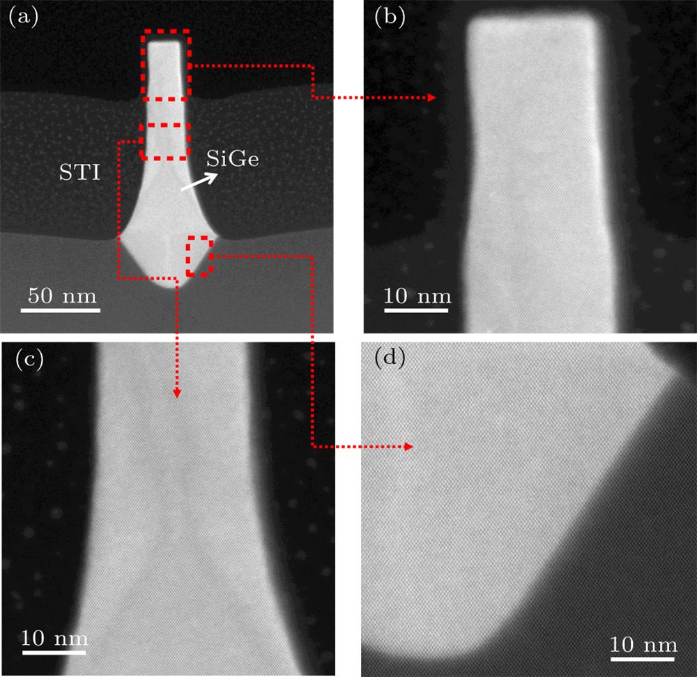
    Fig. 2. HAADF-STEM images for SiGe fin fabrication in narrow trench by using replacement fin strategy, and its high resolution images (a) at top of SiGe fin, (b) in the middle of SiGe fin, and (c) at interface between SiGe and Si substrate.
    (a) TEM and (b) HRSTEM images of SiGe fin along fin direction post SiGe SEG.
    Fig. 3. (a) TEM and (b) HRSTEM images of SiGe fin along fin direction post SiGe SEG.
    SMF images of SiGe SEG from bottom to top along fin direction, for (a) Si substrate, (b) SiGe between STI oxides.
    Fig. 4. SMF images of SiGe SEG from bottom to top along fin direction, for (a) Si substrate, (b) SiGe between STI oxides.
    EELS mapping results for dark area of SiGe fin.
    Fig. 5. EELS mapping results for dark area of SiGe fin.
    HAADF-STEM images for (a) SiGe’s selective epitaxial growth in the narrow trench, and (b) its high resolution image at bottom of SiGe fin.
    Fig. 6. HAADF-STEM images for (a) SiGe’s selective epitaxial growth in the narrow trench, and (b) its high resolution image at bottom of SiGe fin.
    Ying Zan, Yong-Liang Li, Xiao-Hong Cheng, Zhi-Qian Zhao, Hao-Yan Liu, Zhen-Hua Hu, An-Yan Du, Wen-Wu Wang. High crystalline quality of SiGe fin fabrication with Si-rich composition area using replacement fin processing[J]. Chinese Physics B, 2020, 29(8):
    Download Citation