
Ang Li, Jordan Davis, Andrew Grieco, Naif Alshamrani, Yeshaiahu Fainman. Fabrication-tolerant Fourier transform spectrometer on silicon with broad bandwidth and high resolution[J]. Photonics Research, 2020, 8(2): 219
- Photonics Research
- Vol. 8, Issue 2, 219 (2020)
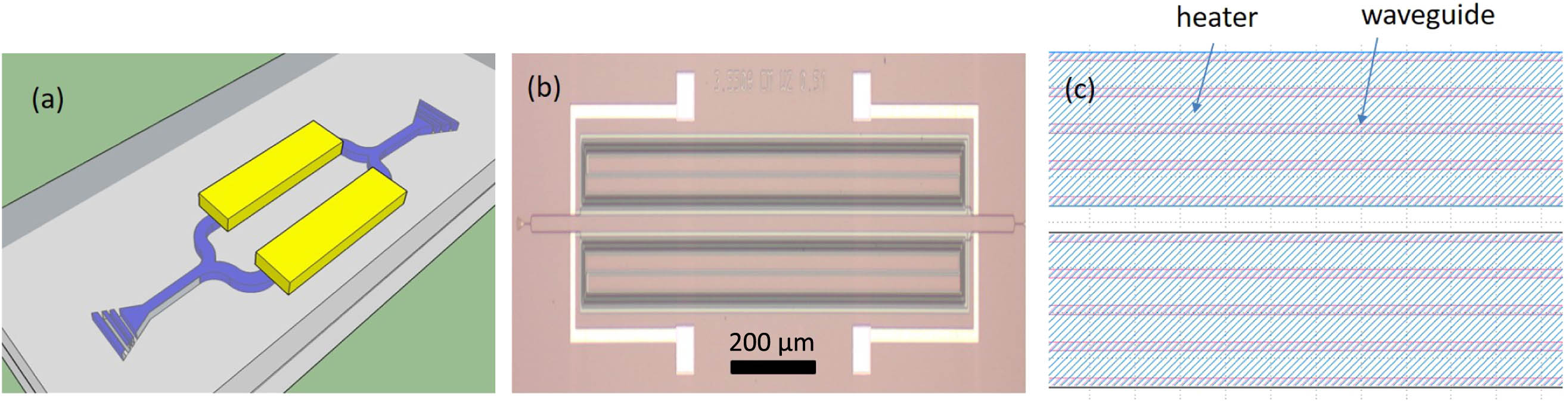
Fig. 1. (a) Schematic and (b) microscopic image of the fabricated device. (c) Zoom view of the waveguides and heater. The waveguide is designed to have a serpentine shape to reduce the footprint, and the heater has a width of 17 μm that covers five waveguides in order to maintain low resistance.
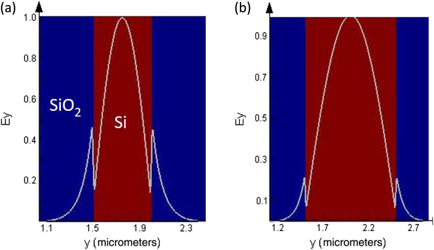
Fig. 2. Simulated E y
Fig. 3. Simulated interferograms and recovered spectra from two different devices: (a), (b) a balanced MZI with waveguide length of 3 cm; (c), (d) a balanced MZI with waveguide length of 10 cm. For both devices, the maximum temperature change is 60 K. Their individual spectral resolutions are 0.42 THz and 0.13 THz, respectively.
Fig. 4. Simulated interferogram and recovered spectrum from two different devices: (a), (b) a balanced MZI with slightly different waveguide widths for the two arms (0.5 μm and 0.52 μm); (c), (d) a balanced MZI with slightly different waveguide widths for the two arms (1 μm and 1.02 μm). The 20 nm width difference corresponds with typical fabrication variation. For both devices, the arm length is 10 cm and maximum temperature change is 60 K.
Fig. 5. Cutback method to characterize two different types of strip waveguides with 0.5 μm width and 1 μm width.
Fig. 6. Experimental results of a balanced FTS with identical arm widths of 1 μm. (a) Raw data of the interferogram as a function of power injection to the heaters. The sign in the x
Fig. 7. Experimental results of impacts of fabrication variation on a balanced FTS. (a), (b) Interferogram and spectrum reconstruction of a balanced FTS with arm widths of 1 μm and 1.02 μm. (c), (d) Interferogram and spectrum reconstruction of a balanced FTS with arm widths of 0.5 μm and 0.52 μm. The 20 nm difference in the two arms represents the fabrication variation in CMOS technology. Clearly, the device using a large waveguide width is tolerant to this amount of variation, while the 0.5 μm device fails to reconstruct the spectrum.

Set citation alerts for the article
Please enter your email address
© Copyright 2018-2021 | Chinese Laser Press. All Rights Reserved 沪ICP备15018463号-20