Ang Li, Jordan Davis, Andrew Grieco, Naif Alshamrani, Yeshaiahu Fainman, "Fabrication-tolerant Fourier transform spectrometer on silicon with broad bandwidth and high resolution," Photonics Res. 8, 219 (2020)
Copy Citation Text
We report an advanced Fourier transform spectrometer (FTS) on silicon with significant improvement compared with our previous demonstration in [Nat. Commun.9, 665 (2018)2041-1723]. We retrieve a broadband spectrum (7 THz around 193 THz) with 0.11 THz or sub nm resolution, more than 3 times higher than previously demonstrated [Nat. Commun.9, 665 (2018)2041-1723]. Moreover, it effectively solves the issue of fabrication variation in waveguide width, which is a common issue in silicon photonics. The structure is a balanced Mach–Zehnder interferometer with 10 cm long serpentine waveguides. Quasi-continuous optical path difference between the two arms is induced by changing the effective index of one arm using an integrated heater. The serpentine arms utilize wide multi-mode waveguides at the straight sections to reduce propagation loss and narrow single-mode waveguides at the bending sections to keep the footprint compact and avoid modal crosstalk. The reduction of propagation loss leads to higher spectral efficiency, larger dynamic range, and better signal-to-noise ratio. Also, for the first time to our knowledge, we perform a thorough systematic analysis on how the fabrication variation on the waveguide widths can affect its performance. Additionally, we demonstrate that using wide waveguides efficiently leads to a fabrication-tolerant device. This work could further pave the way towards a mature silicon-based FTS operating with both broad bandwidth (over 60 nm) and high resolution suitable for integration with various mobile platforms.
1. INTRODUCTION
Fourier transform spectrometers (FTSs) recovering an unknown spectrum are powerful tools in various fields including chemical sensing, bio-medical applications, and autonomous vehicles, etc. [1–4]. Compared to other direct-detection-based spectrometers, such as monochromators or grating-based spectrum analyzers, one of the key advantages of FTSs is Fellgett’s advantage, namely, higher signal-to-noise ratio and dynamic range [5]. The FTS employs an interferogram (i.e., autocorrelation function) generated from the input signal with unknown spectra using an interferometer, where the input signal is divided into two paths with variable optical path difference (OPD). At the output of the interferometer, the optical signals from these two optical paths are recombined on a photodetector, which is used to generate a photocurrent as a function of OPD, thereby generating the desired interferogram. The Fourier transform of the detected interferogram (i.e., autocorrelation function) produces the power spectral density of the input signal. The larger the maximum OPD, the higher the spectral resolution. A classical FTS typically uses a moving element (such as a mirror) to introduce quasi-continuous tunable OPD between two paths and generates a temporal interferogram (i.e., autocorrelation function). Thus, FTSs are usually realized as bulky free-space interferometric systems and suffer from slow scanning speeds, resulting in long measurement times.
Use of silicon photonics as a platform for FTS realization has attracted widespread attention as a candidate to meet the rapidly growing demand for low-cost, portable devices [6]. In contrast to free-space FTSs, most FTSs demonstrated on silicon platforms are spatial heterodyne spectrometers (SHSs) that employ a large array of unbalanced Mach–Zehnder interferometers (MZIs) with varying length differences, each of which introduces a fixed amount of OPD to the spectrum [3,7–9]. In order to achieve high resolution (i.e., large OPD), the incident spectral signal is typically required to be split into over 50 MZIs with predetermined delays, resulting in a considerably large footprint, large insertion loss, low dynamic range, and low signal-to-noise ratio. SHSs also usually support a narrow bandwidth (i.e., a few 100 pm) despite its very high resolution (a few 10s of pm) [7]. An alternative approach, called stationary FTS, generates a spatial interferogram utilizing a standing wave pattern between two co-propagating waves [10]. Compared to the SHS approach, it is demonstrated to trade-off a significantly reduced footprint and broad operating bandwidth (100 nm) for very low resolution (6 nm). Moreover, a dense array of photodetectors is required to be fabricated on top of the structure plane to capture the spatial interferogram, which significantly limits scalability, increases integration complexity, and perturbs the spatial interferogram [10].
Recently, an analogue to classical FTS on silicon that generates a temporal interferogram by quasi-continuously tuning the OPD between two arms of a single MZI was demonstrated [11]. As shown in Fig. 1, tuning of the OPD is achieved by applying electrical power to an integrated heater above the waveguide to create a phase shift using the thermo-optic effect in one of the two MZI arms. To achieve a moderate spectral resolution (3 nm) with a feasible temperature change, the waveguide length was designed to be 3 cm. To keep a compact footprint, the waveguide was designed to have a serpentine geometry. This device was shown to operate with large bandwidth signals (), limited only by the bandwidth of the input coupler of the waveguide and the transmission window of the optical materials. In comparison with SHS and stationary FTS, this temporal heterodyne spectrometer (THS) [11] has the advantages of operation with broad bandwidth signals, compact footprint, high dynamic range, and compatibility with chip-scale integration, making it a promising candidate for portable, broadband, low-cost FTSs. A major disadvantage of TSH lies in the demonstrated spectral resolution (so far, 3 nm or 0.38 THz), which is insufficient for many applications, and the research to tackle this problem remains scarce. In theory, the resolution of a single THS could be increased by supplying higher power to the heater or implementing a longer waveguide, which are both non-trivial approaches for centimeter (cm)-scale waveguides. High power injection to the heaters will aggravate thermal structural expansion, raise the risk of shortening the device lifetime, and jeopardize heater integrity. Other disadvantages include large resistance (over 10 kΩ) for long heaters, making them impractical to operate at high electrical power, whereas longer waveguides will affect and limit the sensing dynamic range and the signal-to-noise ratio. Alternatively, the resolution could be improved using a circuit-level technique by deploying a silicon microring resonator in front of the THS that selectively sends a narrow band of the incident signal to the THS for processing [12]. The resolution is improved to 0.47 nm, but this technique is very similar to those direct-detection approaches that sacrifice the SNR of the THS.
Sign up for Photonics Research TOC. Get the latest issue of Photonics Research delivered right to you!Sign up now
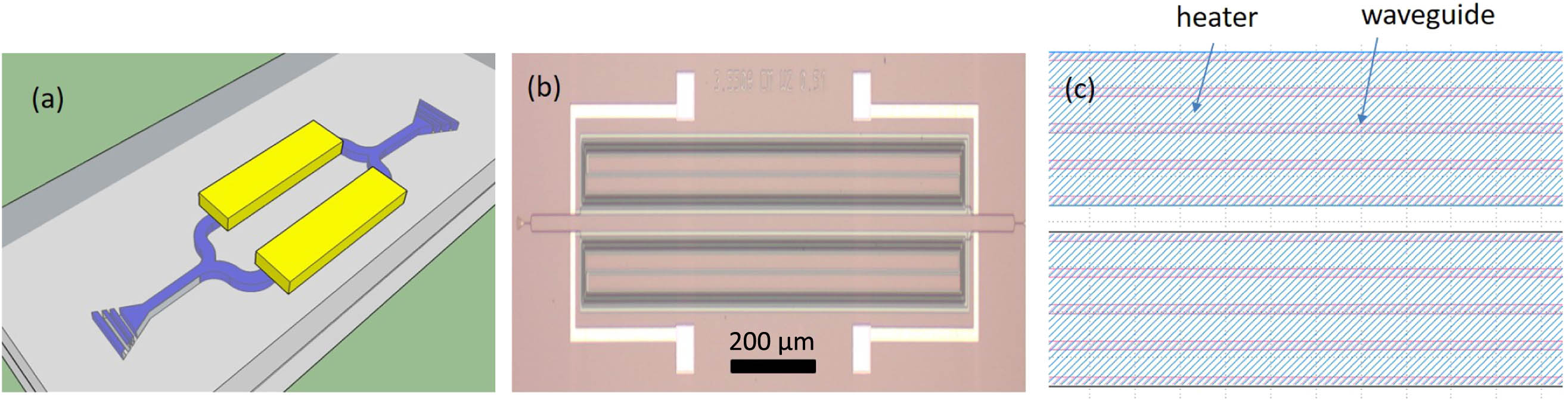
Figure 1.(a) Schematic and (b) microscopic image of the fabricated device. (c) Zoom view of the waveguides and heater. The waveguide is designed to have a serpentine shape to reduce the footprint, and the heater has a width of 17 μm that covers five waveguides in order to maintain low resistance.
In this paper, by engineering the waveguides to reduce propagation loss and optimizing the heater design to accommodate higher power actuation, we demonstrate a higher spectral resolution THS [11]. The device utilizes broader multi-mode waveguides in the straight section of the serpentine waveguide to reduce the propagation loss while reducing the waveguide width at bending sections to 500 nm to avoid modal crosstalk and retain a compact footprint. With the reduction of propagation loss, the serpentine waveguide length is increased from 3 cm in THS from Ref. [11] to 10 cm, and the heater design is improved so that the total resistance is reduced to around 5 kΩ, compared to 15 kΩ in Ref. [11] with more coverage of the waveguides. This technique has been applied in other applications such as high- resonator and microwave filters [13,14], but we realize that there is a prolific body of work in spectrometers in which this technique is not used [3,7,9,12,15]. Our experiments demonstrate a spectral resolution of 0.11 THz or sub-nanometer (nm), more than 3 times higher than that in the previous demonstration [11] while maintaining a broad bandwidth of operation with a compact footprint. Moreover, we investigate and prove, through both simulations and experimental results, that fabrication variations imposed on standard single-mode waveguides degrade the performance of silicon THS or even deteriorate their functionality, while using wide waveguides in the MZI arms of the current design not only reduces optical loss but also significantly reduces the effect of fabrication errors.
2. DEVICE DESIGN AND SIMULATION
As discussed in Section 1, to increase the spectral resolution of FTSs, the maximum achieved OPD should be increased using longer waveguides. Conversely, longer waveguides result in a higher signal insertion loss, which decreases the dynamic range of the device. To maintain a high dynamic range, the propagation loss needs to be reduced. The main source of losses in silicon waveguides is due to scattering on the waveguide-sidewall roughness, which is inevitable due to the limitations of current fabrication technology [16,17]. A typical electric field distribution for TE-like propagating mode in a 500 nm wide and 220 nm high silicon waveguide is shown in Fig. 2(a). It is evident that a strong electric field on the waveguide sidewalls will interact with its roughness and excite undesired unguided modes (radiative loss) or back-propagating modes (stochastic backscattering). Besides, a long-silicon-strip waveguide has been reported to exhibit extremely strong fluctuations in its transmission spectrum, which is also attributed to sidewall roughness [18]. One effective technique to reduce the roughness-induced issues is to reduce the electric field amplitude on the waveguide sidewalls by using a wide waveguide [see Fig. 2(b)]. We use this approach in our FTS serpentine arm design to reduce the losses and increase its length. Specifically, the straight sections of the serpentine arm are engineered to be μ cross-section strip waveguides with low propagation loss, whereas the bending sections are implemented using strip waveguides with a cross section to avoid excitation of unwanted higher-order modes and also keep a tight bend radius (i.e., 5 μm) with negligible bending loss [19]. The transition between the multi-mode and single-mode waveguides is achieved using an adiabatic linear taper with a length of 4 μm that exhibits negligible loss and reflection.
Figure 2.Simulated intensity of the TE mode in (a) a 0.5 μm wide waveguide and (b) a 1 μm wide waveguide. The thickness is 220 nm.
In this low-loss design, we also increased the serpentine waveguide length to 10 cm, such that at the same temperature change, we could expect more than 3 times increase in OPD compared to that used in Ref. [11], which will result in about 3 times increase in resolution. Also, the corresponding serpentine heater benefits from the improved design to more efficiently cover the waveguides while keeping the total resistance down to a few kΩ, making it suitable for operation with our voltage source, which is limited to 210 V. The serpentine heater has a width of 17 μm and a total length of 2.3 cm covering the entire 10 cm long waveguide [shown in Fig. 1(c)]. The simulated performance of the FTS with 3 cm long arms and 10 cm long arms is plotted in Figs. 3(a)–3(d). Given the same temperature change of 60 K, the current 10 cm device leads to a spectral resolution of 0.14 THz, which is more than 3 times higher than that obtained with the 3 cm device.
Figure 3.Simulated interferograms and recovered spectra from two different devices: (a), (b) a balanced MZI with waveguide length of 3 cm; (c), (d) a balanced MZI with waveguide length of 10 cm. For both devices, the maximum temperature change is 60 K. Their individual spectral resolutions are 0.42 THz and 0.13 THz, respectively.
Besides the enhancement of spectral resolution, another issue that has been neglected is fabrication variation on the waveguide width. In the work reported in Ref. [11], the center of the interferogram is shifted to 0.172 ps due to the fabrication-variation-induced differences in the two arms. The FTS works, as the variation is relatively small such that the temperature change caused by the heater (55 K) could make the device meet a zero-OPD (center of the interferogram) condition. However, the device was fabricated using electron beam lithography, which induces smaller variations in waveguide dimensions compared to optical lithography, which is the main choice for CMOS foundries. Moving towards a mature THS-on-silicon platform, the fabrication variation should be thoroughly studied and taken into consideration. According to wafer-scale characterization of manufacturing variability for silicon photonics components [20], the typical width variation in a strip waveguide can be as large as 20 nm. To study the impacts of such a large fabrication variation, a series of simulations were performed for two devices: an MZI with waveguide widths of 0.5 μm and 0.52 μm and an MZI with widths of 1 μm and 1.02 μm. For both devices, the arm length is 10 cm and the maximum temperature change is 60 K. The results are plotted in Fig. 4. Compared to the imperfection-free device, shown in Figs. 3(c) and 3(d), the interferogram of the device with 0.5 μm and 0.52 μm waveguide widths does not contain the zero-OPD information, and thus the spectrum reconstruction fails [Figs. 4(a) and 4(b)]. This is due to a 20 nm variation in the 500 nm waveguide width, which translates to an effective index difference of 0.02. A 60 K temperature change only induces a index change of 0.01 and thus cannot compensate for this index difference. On the other hand, using wide waveguides with 1 μm width, with the same fabrication variation present, the effective index difference is as small as 0.003. Consequently, the interferogram shifts away from the origin but still contains the zero-OPD information, and thus the spectrum can be successfully reconstructed [Figs. 4(c) and 4(d)].
Figure 4.Simulated interferogram and recovered spectrum from two different devices: (a), (b) a balanced MZI with slightly different waveguide widths for the two arms (0.5 μm and 0.52 μm); (c), (d) a balanced MZI with slightly different waveguide widths for the two arms (1 μm and 1.02 μm). The 20 nm width difference corresponds with typical fabrication variation. For both devices, the arm length is 10 cm and maximum temperature change is 60 K.
The devices were fabricated through a multi project wafer (MPW) service at a commercial foundry (Applied Nanotools) with electron beam lithography, and thus the fabrication variation in the waveguide width becomes negligible compared to our intentional variation of 20 nm. Grating couplers are employed as the fiber/chip coupling components. Characterization of waveguide propagation loss with widths of 0.5 μm and 1 μm is given in Fig. 5. All waveguides have the same serpentine type as used in our THS. Clearly, for our 10 cm long FTS, using 1 μm wide waveguides could increase the dynamic range about 8.5 dB. The measured heater resistance is about 5 kΩ.
Figure 5.Cutback method to characterize two different types of strip waveguides with 0.5 μm width and 1 μm width.
Following the calibration procedures reported in Ref. [11], we aim at reconstructing the spectrum of an ASE source (C+L band). The results of a perfectly balanced FTS (1 μm arm width and 10 cm arm length) are plotted in Fig. 6. In Fig. 6(a), the raw data of the measured interferogram as a function of power injection to the heaters is present. The positive/negative sign of the axis refers to actuation of the top/bottom heater. The raw data exhibits a modulated envelope due to the thermally induced chip expansion that modifies the grating coupler performance and thus the overall coupling efficiency. The maximum power injection is about 5.2 W, corresponding with a voltage supply at 160 V. Even though our equipment can deliver voltage up to 210 V, the strong thermally induced chip expansion decreased the power collected by the photodetector to noise floor levels as evident in Fig. 6(a). The post-processed inteferogram [Fig. 6(b)] is almost centered at zero OPD, indicating negligible fabrication variation between the two arms. The reconstructed spectrum matches with the original spectrum well [Fig. 6(c)] with a spectral resolution around 0.11 THz [Fig. 6(d)], more than 3 times enhancement compared to the previous demonstration [11]. The resolution could be further improved by injecting more power into the device once the thermally induced expansion is resolved. The small discrepancy between the retrieved spectrum and the input spectrum shown in Fig. 6(b) is a result of multi-source instabilities during the measurement procedure. For instance, the input and output fibers can show certain drift during the 1.5 h long measurement period, which leads to slightly inaccurate optical power collected by the detector. Also, in the current setup, the electrical probes are attached to the electrical pads without firm bonding. Therefore, during the measurement period, especially at high power injection to the heater, the thermal expansion might cause the contact between the probes and the on-chip pads to become unstable, resulting in inaccurately monitored power injection to the heaters. All these minor issues could be effectively solved once the chip is packaged, such that the fibers and electrical probes would be firmly attached to the silicon chip during the measurement.
Figure 6.Experimental results of a balanced FTS with identical arm widths of 1 μm. (a) Raw data of the interferogram as a function of power injection to the heaters. The sign in the axis refers to the actuation of different heaters. (b) Plot of the post-processed interferogram ready for Fourier transformation. (c) The reconstructed spectrum compared with the original input spectrum.
The experimental results of the fabrication-tolerant device are given in Fig. 7. Figures 7(a) and 7(b) show the interferogram and spectrum reconstruction of a balanced FTS with arm widths of 1 μm and 1.02 μm, while the interferogram and spectrum reconstruction of a balanced FTS with arm widths of 0.5 μm and 0.52 μm are plotted in Figs. 7(c) and 7(d). The 20 nm difference in the two arms represents the fabrication variation in CMOS technology. For 1 μm waveguide, this amount of width variation leads to a much smaller effective index change (around 0.003 based on simulations), and the interferogram still contains the zero-OPD regime; thus, the spectrum could be successfully reconstructed. For the device with 0.5 μm width, 20 nm variation in the waveguide width could completely shift the zero OPD out of the measured interferogram, resulting in a failure in spectrum reconstruction.
Figure 7.Experimental results of impacts of fabrication variation on a balanced FTS. (a), (b) Interferogram and spectrum reconstruction of a balanced FTS with arm widths of 1 μm and 1.02 μm. (c), (d) Interferogram and spectrum reconstruction of a balanced FTS with arm widths of 0.5 μm and 0.52 μm. The 20 nm difference in the two arms represents the fabrication variation in CMOS technology. Clearly, the device using a large waveguide width is tolerant to this amount of variation, while the 0.5 μm device fails to reconstruct the spectrum.
In this paper, we report our follow-up work in silicon FTSs with a focus on resolution enhancement and fabrication tolerance. By using hybrid waveguides in the serpentine section with reduced propagation loss and improved heater design, the maximum achievable OPD between the two arms is increased, leading to increased resolution, which is confirmed by experimental data: 0.11 THz resolution is achieved compared to the previous demonstration of a resolution of 0.38 THz [11]. Also, for the first time to our knowledge, we draw the attention to the impacts of fabrication variation on this kind of device and demonstrate that using our technique could make the device tolerant enough for CMOS technology, paving the way for a commercial product.
[18] A. Li, Y. Xing, R. Van Laer, R. Baets, W. Bogaerts. Extreme spectral transmission fluctuations in silicon nanowires induced by backscattering. 13th International Conference on Group IV Photonics (GFP), 160-161(2016).
Ang Li, Jordan Davis, Andrew Grieco, Naif Alshamrani, Yeshaiahu Fainman, "Fabrication-tolerant Fourier transform spectrometer on silicon with broad bandwidth and high resolution," Photonics Res. 8, 219 (2020)