
Yinsheng Peng, Shufeng Gong, Kai Liu, Minghai Yao. Nano-sphere surface arrays based on GaAs solar cells[J]. Journal of Semiconductors, 2020, 41(1): 012701
- Journal of Semiconductors
- Vol. 41, Issue 1, 012701 (2020)
Abstract
1. Introduction
The GaAs semiconductor material has been known as one kind of important optoelectronic materials that provides direct band gap energy and high mobility carrier properties. Therefore, the material is commonly used to fabricate high conversion efficiency solar cells and have also been attracted much attention in recent years because of their high conversion efficiency compared to the other solar cells[
It is well known that surface texturing can be utilized to improve the conversion efficiency of the solar cells. By introducing surface texture, it results in the reduced reflection losses, enhanced light scattering and diffraction of light in the solar cells. Recently, the surface texturing technique has widely been utilized in the fabrication of silicon based solar cells with various designs such as honeycomb, pyramid, invert-pyramid, and V-trench structures[
In general, the antireflection coatings with single, double and triple layers at the top have been used for light trapping in the GaAs solar cells[
This motivated us to concentrate our work on studying surface texturing atop of GaAs solar cells. We found that an alternative solution is to deposit a nano-sphere array with periodic structure using different material by self-assembly method on the surface of GaAs, the light path length can be significantly increased based on the scatting of the nano-spheres and the diffraction of photonic crystals. It should be note that the self-assembly is one of the simplest methods building a two-dimension periodic structure. Furthermore, the light trapping structure has the advantage that the geometrical parameters could be easily varied and the whole structure are easily to be engineered, rescale and reproduce, which is also one of the key motivation for this work. To date, single-junction GaAs solar cells with a self-assembly micro-sphere arrays deposited on the front surface of GaAs solar cells, micro-sphere diameter of 1 μm and the refractive index of 1.59, have been reported to have an relatively increased conversion efficiency of 25% experimentally[
In this work, we present our efforts on simulating and analyzing the effect of two-dimensional nano-sphere surface array on the characteristic of GaAs solar cells based on the scattering and diffraction theory of the nano-spheres photonic crystals[
2. Solar cell structure
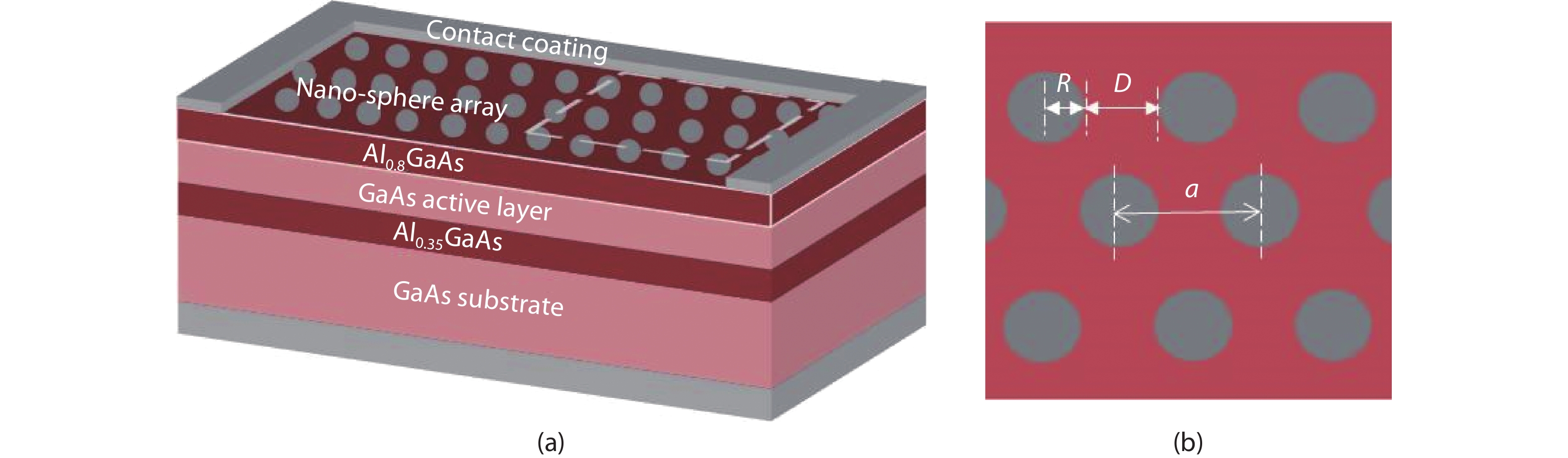
The proposed surface nano-sphere light trapping structure based on thin film GaAs solar cells has been shown schematically in Fig. 1. The structure consists of a nano-sphere surface coating layer, an Al0.8GaAs window layer, and active layer of GaAs is placed below this window layer. An Al0.35GaAs back window layer is placed below the active layer followed by the Al back reflector. Top contact electrodes are also employed as Fig. 1. The wavelength dependent material parameters are considered for GaAs and AlGaAs[
![]()
Figure 1.(Color online) (a) Schematic of the GaAs solar cell with nano-sphere array in side view. (b) Schematic top view of the nano-sphere surface array.
The active material layer has been kept fixed at a particular thickness (here including a 0.5 μm p-GaAs emitter layer, 3 μm n-GaAs base and 350 μm GaAs substrate layer). The front and back window layer of Al0.85GaAs and Al0.35GaAs has been set to 0.03 and 0.01 μm, respectively, as thicker window layer might degrade the performance of the device[
The nano-sphere array at the top is assumed to be a two-dimensional hexagonal lattice arrangement, as it would provide better diffraction as compared to the square array. As mentioned previously, the condition is similar to the diffraction grating, the role of the nano-spheres array is to deflect the normally incident light to the oblique direction and the diffracted waves propagates at nearly grazing angle within the solar cells, thus improves light propagate paths within the absorption layer. Thin AlGaAs window layers with higher band gap and heavily doped serve an important role to deflect minority carriers away from the contacts in order to reduce surface recombination[
In our article, the optical performance of the solar cell has been analyzed through calculating absorption in the active area and reflection from the top surface through power conversion efficiency and I–V curve simulations. The optical absorption in the solar cells is calculated using the scattering matrix method[
The calculated total absorption in GaAs layer is weighted by the air mass (AM) 1.5 solar spectrum and integrated from 400 nm (λmin) to 900 nm (λmax) to obtain the average absorption
And short-circuit current density,
where e is the electron charge, h is Planck constant, c is the light speed in vacuum, and
where
3. Results and discussion
It must be noted that the nano-sphere coating have to be a monolayer to avoid the effects of the photonic crystalline band gap which would interfere with the absorption of the solar cell[
![]()
Figure 2.(Color online) The conversion efficiency as a function of radius for different
![]()
Figure 3.(Color online) Calculated spectral distribution graph for (a) absorption, (b) reflection and (c) transmission for different
In addition, a series of diffraction peaks are observed, which due to diffraction resonances generated from the electromagnetic waves internally reflected at the surfaces of the wafer when the phase difference between modes reflected from the front and rear surfaces are multiples of
For a triangular lattice, reciprocal lattice vector G has components of
Next, taken the influence of nano-sphere size on the performance of solar cells, Fig. 2 shows that the significant high conversion efficiency (> 20.6%) is observed in the nano-sphere radius variation range from 0.3 to 1.2μm, keeping the distance of adjacent nano-sphere (D) of 0 μm. In addition, for the optimal D of 0 μm, it is found that the conversion efficiency started to rapidly increase and nearly varies linearly from 16.4% to 20.8% when the radius increases from 0 to 0.5 μm. However, the conversion efficiency exhibits very slight variation (around 0.2%) in the wide radius range of 0.5–1.2 μm, then the conversion efficiency started to dip exponentially as the radius of > 1.2 μm and drops below 18% when the radius is of > 2.2 μm. Fig. 4 shows the contour map for photon absorption between radius and wavelength with D of 0 μm. The dense absorption peaks are observed when the nano-sphere radius varies from 0.3 to 1.2 μm in the wavelength range of 0.4–0.85 μm, resulting in enhancement absorption and high conversion efficiency. However, when the radius of the nano-sphere is greater than 1.5 μm or less than 0.3 μm, the absorption peaks significantly becomes sparse, thus resulting in low conversion efficiency. The could be further confirmed by the absorption, reflection and transmission spectra of solar cells, as seen in Fig. 5. From the figure, it is found that the absorption enhancement with the reduction of nano-sphere radius (seen in Fig. 5(a)), which is mainly responsible for reducing of reflection on the surface of solar cells (seen in Fig. 5(b)) and the much low transmission in the wavelength ranges of 0.4–0.85 μm, as shown in Fig. 5(c).
![]()
Figure 4.(Color online) Shows the contour map for photon absorption between radius and wavelength with
![]()
Figure 5.(Color online) Calculated spectral distribution graph for (a) absorption, (b) reflection and (c) transmission for different
It is interested to find that the extremely weak photon absorption is observed in long wavelength range of 0.85–0.9 μm regardless of nano-sphere R and D, as shown in Fig. 3(a) and Fig. 5(a). This is due to the enhancement of reflection and transmission from the solar cells in the long wavelength range. The significant diffraction resonance occur is required that the photonic crystal period (indicated by
Then, we calculated the influence of nano-sphere refractive index on the conversion efficiency keeping the D and R of 0 and 0.6 μm, respectively, as seen in Fig. 6. The conversion efficiency rapidly increases as the refractive index variation from 1.2 to 1.8, and the higher conversion efficiency can be observed in the refractive index variation range of 1.8–2.2, then the conversion efficiency slowly reduces when the refraction index increases from 2.2 to 3.0. Fig. 7 illustrates the J–V characteristic of optimal GaAs solar cells with distance of adjacent nano-spheres (D), radius (R) and refractive index (n) of 0 μm, 0.6 μm and 2.1, respectively.
![]()
Figure 6.Illustration of the overall cell efficiency as a function of the refractive index of nano-spheres (
![]()
Figure 7.
Finally, we discuss the tolerance for the three parameters of D, R and n of nano-spheres. It is clearly found from the Fig. 2 that the much poor tolerance is exhibited for the D variation; the conversion efficiency reduces from 20.8% to 18.4% as D increase from optimal value (0 μm) to 1 μm with optimal radius of 0.6 μm, leading to absolute efficiency reduction of 2.4%. However, in the actual fabrication process tightly clustered 2D polymer nano-sphere arrays can be easier to implement using self-assembled manufacture techniques. Fig. 2 also shows that the absolute cell efficiency is varied by less than 1% as the value of R for optimal structure (dark blue line as shown) varies from 0.3 to 1.2 μm, meaning very good manufacturing tolerance. From Fig. 6, it can be found that there is good tolerance for conversion efficiency around the optimal value of refractive index and there is less than 0.2% variation in final cell conversion efficiency for around
It should be noted that the highly order two-dimensional nano-sphere array structures could be fabricated on the top surface of GaAs solar cell using monodisperse polystyrene (PS), PS spheres were synthesized with different sizes via emulsion polymerization at different temperature. The refractive index of the PS nano-spheres is around 1.59 at a wavelength of 550 nm, which is suitable for high-throughput and large-area processing by using self-assembled chemical methods[
4. Conclusion
In this paper, we present our efforts on simulating and analyzing the light trapping in GaAs solar cells using a nano-sphere array surface texture due to the simplest and the fastest methods building a two-dimensional photonic crystal structure on the GaAs surface. Based on the scattering and diffraction theory of the photonic crystals, the simulation results show that the distance of adjacent nano-spheres has the great influence on the conversion efficiency and exhibits poor tolerance, the absolutely conversion efficiency is reduced by exceeding of 2% as the D varies from 0 to 1 μm. In addition, the lower conversion efficiency (< 18%) is exhibited and almost remains unaltered when theD is of > 2 μm. The radius (R) of nano-spheres demonstrates much great tolerance. For D = 0, the solar cells exhibit high conversion efficiency (> 20%) and the efficiency is only varied by less than 1% whenR is varied in a very wide region of 0.3–1.2 μm. One can also find out that there is good tolerance for efficiency around the optimal value of refractive index (n) and there is only about 0.2% decrease in final cell efficiency for around ±24% variation in the optimal values, which implying that it does not demand high precision processing equipment and the whole nano-sphere array could be fully complemented using self-assembled chemical methods.
Acknowledgements
The authors would like to thank National Nature Science Foundation of China (Grant No. 61871350) and Zhejiang Provincial Department of Education for their financial support of this research (Grant Nos. Y201121882 and Y201225406).
References
[1] T Kitatani, Y Yazawa, S Watahiki et al. Optimal growth procedure of GaInP/GaAs heterostructure for high-efficiency solar cells. Sol Energy Mater Sol Cells, 50, 221(1998).
[2] T Takamoto, M Yamaguchi, S Taylor et al. Radiation resistance of high-efficiency InGaP/GaAs tandem solar cells. Sol Energy Mater Sol Cells, 58, 265(1999).
[3] I Garcia, B Rey-Stolle, C Galiana et al. A 32.6% efficient lattice-matched dual-junction solar cell working at 1000 suns. Appl Phys Lett, 94, 053509(2009).
[4] J H Zhao, A H Wang, M A Green et al. 19.8% efficient “honeycomb” textured multicrystalline and 24.4% monocrystalline silicon solar cells. Appl Phys Lett, 73, 1991(1998).
[5] M Tao, W D Zhou, H J Yang et al. Surface texturing by solution deposition for omnidirectional antireflection. Appl Phys Lett, 91, 081118(2007).
[6] V Y Yerokhov, R Hezel, M Lipinski et al. Cost-effective methods of texturing for silicon solar cells. Sol Energy Mater Sol Cells, 72, 291(2002).
[7] R Dewan, M Marinkovic, R Noriega et al. Light trapping in thin-film silicon solar cells with submicron surface texture. Opt Express, 17, 23058(2009).
[8] J Zhao, A Wang, P Altermatt et al. Twenty-four percent efficient silicon solar cells with double layer antireflection coatings and reduced resistance loss. Appl Phys Lett, 66, 3636(1995).
[9] M A Green. Two new efficient crystalline silicon light-trapping textures. Prog Photovolt Res Appl, 7, 317(1999).
[10] N D Lam, Y Kim, K Kim et al. Improved optical absorption and photocurrent of GaAs solar cells with hexagonal micro-hole array surface texturing. J Cryst Growth, 370, 244(2013).
[11] S Chattopadhyay, Y F Huang, Y J Jen et al. Anti-reflecting and photonic nanostructures. Mater Sci Eng R, 69, 1(2010).
[12] B Yan, J M Owens, C Jiang et al. High-efficiency amorphous silicon alloy based solar cells and modules. Proc MRS Symp, 862(2005).
[13] J Springer, A Poruba, L Müllerova et al. Absorption loss at nanorough silver back reflector of thin-film silicon solar cells. J Appl Phys, 95, 1427(2004).
[14] E Yablonovitch, G D Cody. Intensity enhancement in textured optical sheets for solar cells. IEEE Trans Electron Devices, 29, 300(1982).
[15] M A Green. Lambertian light trapping in textured solar cells and light-emitting diodes: Analytical solutions. Prog Photovolt Res Appl, 10, 235(2002).
[16] P Campbell, M A Green. Light trapping properties of pyramidally textured surfaces. J Appl Phys, 62, 243(1987).
[17] J N Munday, H A Atwater. Large integrated absorption enhancement in plasmonic solar cells by combining metallic gratings and antireflection coatings. Nano Lett, 11, 2195(2011).
[18] J Krc, G Cernivec, A Campa et al. Optical and electrical modeling of Cu(In, Ga)Se2 solar cells. Opt Quantum Electron, 38, 1115(2006).
[19] D Zhou, R Biswas. Photonic crystal enhanced light-trapping in thin film solar cells. J Appl Phys, 103, 093102(2008).
[20] T H Chang, P H Wu, S H Chen et al. Efficiency enhancement in GaAs solar cells using self-assembled microspheres. Opt Express, 17, 6519(2009).
[21] C Sun, P Jiang, B Jiang. Broadband moth-eye antireflection coatings on silicon. Appl Phys Lett, 92, 061112(2008).
[22] C K Huang, K W Sun, W Chang. Efficiency enhancement of silicon solar cells using a nano-scale honeycomb broadband anti-reflection structure. Opt Express, 20, A85(2012).
[23] S Domınguez, O Garcıá, M Ezquer et al. Optimization of 1D photonic crystals to minimize the reflectance of silicon solar cells. Photonics Nanostruct: Fundam Appl, 10, 46(2012).
[24] M Tsai, P Tseng, H Chen et al. Enhanced conversion efficiency of a crystalline silicon solar cell with frustum nanorod arrays. Conference on Lasers and Electro-Optics: Laser Science to Photonic Applications(2011).
[25] N Yamada, O N Kim, T Tokimitsu et al. Optimization of anti-reflection moth-eye structures for use in crystalline silicon solar cells. Prog Photovolt Res Appl, 19, 134(2011).
[26] D E Aspnes, S M Kelso, R A Logan et al. Optical properties of Al
[27] A D Rakic, A B Djurišic, J M Elazar et al. Optical properties of metallic films for vertical-cavity optoelectronic devices. Appl Opt, 37, 5271(1998).
[28] Y Mir, A Amine, M Bouabdellaoui et al. The window layers effect on the hardness improvement of space solar cells exposed to the 1 MeV electron irradiations. Opt Quantum Electron, 45, 1189(2013).
[29] N D Gupta, V Janyani. Optical and electrical simulation studies of light trapping in GaAs thin film solar cells using 2D photonic-crystal. J Nanoelectron Optoelectron, 11, 368(2016).
[30] X Wang, M Khan, J L Gray et al. Design of GaAs solar cells operating close to the Shockley-Queisser limit. IEEE J Photovolt, 3, 737(2013).
[31] R Biswas, C G Ding, I Puscasu et al. Theory of subwavelength hole arrays coupled with photonic crystals for extraordinary thermal emission. Phys Rev B, 74, 045107(2006).
[32] Z Y Li, L L Lin. Photonic band structures solved by a plane-wave-based transfer-matrix method. Phys Rev E, 67, 046607(2003).
[33]
[34] N Gupta, V Janyani. Design and optimization of photonic crystal diffraction grating based efficient light trapping structure for GaAs thin film solar cell. J Nanoelectron Optoelectron, 11, 407(2016).
[35] P Bermel, C Luo, L Zeng et al. Improving thin-film crystalline silicon solar cell efficiencies with photonic crystals. Opt Exp, 15, 16986(2007).
[36] N P Gupta, V Janyani. Design and analysis of light trapping in thin film GaAs solar cells using 2-D photonic crystal structures at front surface. IEEE J Quantum Electron, 53, 1(2017).

Set citation alerts for the article
Please enter your email address
© Copyright 2018-2021 | Chinese Laser Press. All Rights Reserved 沪ICP备15018463号-20