• Infrared and Laser Engineering
  • Vol. 50, Issue 1, 20211013 (2021)
Lijing Yu1、2、3, Libin Tang1、2、3, Wenyun Yang2, and Qun Hao1
Author Affiliations
  • 1The Laboratory of Photonics Information Technology, Ministry of Industry and Information Technology, School of Optics and Photonics, Beijing Institute of Technology, Beijing 100081, China
  • 2Kunming Institute of Physics, Kunming 650223, China
  • 3Yunnan Key Laboratory of Advanced Photoelectric Materials & Devices, Kunming 650223, China
  • show less
    DOI: 10.3788/IRLA20211013 Cite this Article
    Lijing Yu, Libin Tang, Wenyun Yang, Qun Hao. Research progress of uncooled infrared detectors(Invited)[J]. Infrared and Laser Engineering, 2021, 50(1): 20211013 Copy Citation Text show less
    [in Chinese]
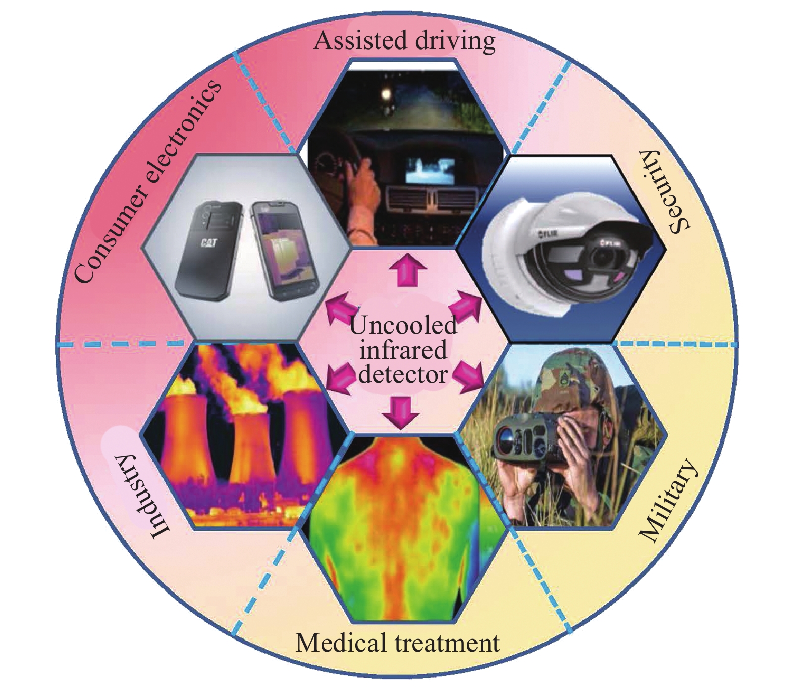
    Fig. 1. [in Chinese]
    [in Chinese]
    Fig. 2. [in Chinese]
    [in Chinese]
    Fig. 3. [in Chinese]
    [in Chinese]
    Fig. 4. [in Chinese]
    [in Chinese]
    Fig. 5. [in Chinese]
    [in Chinese]
    Fig. 6. [in Chinese]
    Package typeFeatureMajor manufacturersProduct
    Metal packageHigh cost, difficult to achieve civilian use when applied in the military field, and will gradually fade out Early ULIS, DRS, SCD, NEC, BAE
    Ceramic packageUpgraded form of metal packaging, using cheap ceramic materials, reducing packaging volume and weight, and reducing packaging costs The most popular packaging technology in recent years
    Wafer level packageHigh integration, simplified process steps, suitable for mass production and low cost production FLIR, ULIS, Guide infrared, Iray
    Pixel level packageSimplifies the manufacturing process of uncooled IRFPA, reducing packaging costs to the extreme This technology is still in the research stage
    Table 1. [in Chinese]
    ManufacturerThermal materialPixel size/µmArray scale Package formNETDRef.
    FLIR (US) VOx1280×60/160×120Metal/ Ceramic / Wafer level<50 mK[24]
    640×512/320×256<40 mK;<50 mK; <60 mK
    17336×256<30 mK
    DRS (US) VOx171024×768/640×480/320×240Metal/ Ceramic≤14 ms /<40 mK[25]
    640×480≤14 ms /<50 mK
    Lynred (France) α-Si 12640×480;Wafer level<10 ms /<60 mK[26]
    320×240Ceramic<10 ms /<60 mK
    171024×768;Wafer level<12 ms /<50 mK
    640×480;Ceramic<12 ms /<50 mK;<40 mK; <30 mK;
    384×2880×120<10 ms /<60 mK
    SCD (Israel) VOx171024×768/12 ms/<45 mK[27]
    640×512;Ceramic//<35 mK
    640×480Ceramic10-18 ms/ 22-50 mK
    Iray (China) VOx121280×1024;640×512Wafer level/Ceramic7 ms;10 ms /≤40 mK;≤50 mK[28]
    141024×768;640×512Ceramic7 ms /≤40 mK
    17640×512;384×288Metal10 ms /≤50 mK
    384×288Wafer level/Ceramic10 ms /≤40 mK
    DALI (China) α-Si 151 920×1080, 1280×1024, 1024×768Metal≤50 mK[29]
    17160×120, 240×180,384×288, 640×480Ceramic≤60 mK
    384×288Metal≤50 mK
    2580×80, 120×120, 160×120Ceramic≤50 mK
    384×288Metal≤40 mK
    Guide infrared (China) VOx12640×512;400×300;256×192;Wafer level<12 ms/<40 mK;<60 mK[30]
    1280×1024;640×512;400×300;256×192;Metal<12 ms/<30 mK;<40 mK;<60 mK
    17400×300;120×90Wafer level<12 ms/<40 mK
    400×300;800×600Metal<12 ms/<40 mK
    GWIC (China) VOx20640×512;Metal≤12 ms/≤40 mK;≤60 mK[31]
    17≤12 ms/≤40 mK;≤50 mK
    17384×288≤12 ms/≤40 mK;≤50 mK
    2015 ms/≤40 mK;≤50 mK
    25≤10 ms/≤40 Mk;≤50 mK
    Table 2. [in Chinese]
    MaterialMaterial characteristics or functionsDevice typeDevice performanceRef.
    SiliconVery low power consumptionCMOS-SOI-NEMSReduced power consumption and highly adaptable [43]
    VOx+Au Enhanced absorptionBolometerAt wavelengths λ =4.8 µm and λ =9 µm with the absorption magnitudes more than 0.98 and 0.94; tunable dual-band absorption peaks can be achieved. [44]
    VOx+Au Modulation wavelengthBolometerThe peak wavelength can be tailored from 2.4 to 10.2 µm. [45]
    α-Si +Au Enhanced absorptionBolometerNEP:100 pW/Hz1/2D*>5×107 Jones [46]
    SiUltra-thin, highly-dopedBolometerFast and highly-sensitive[47]
    Polycrystalline films of Mn-Co-Ni-OHigh TCR, low excess noiseBolometerAt 30 Hz, noise equivalent temperature: 2.1 × 10⁻⁷ K/Hz1/2, responsivity: 330 V/W, detectivity: 0.6 × 108 cm Hz1/2/W, noise equivalent power: 3.7 × 10⁻¹⁰ W/Hz1/2[48]
    SixGeyO1−xyHigh TCR and a low corresponding resistivity can be achieved using various compositions. BolometerTCR: −3.95%/K, the TCR can be increased and resistivity can be decreased by optimizing the film contents at low oxygen concentration [49]
    GrapheneWith a variety of reported photodetectors ranging from visible to THz frequencies BolometerTCRs up to 900%/K, and the ability to resolve temperature variations down to 15 µK. [50]
    GrapheneCan be synthesized inexpensively via a non-toxic process PhotodetectorModulates the back-gate voltage to increase the photoresponse by a factor of approximately 600 compared to that for a conventional graphene photodetector. [51]
    HgTe CQDTunable optical response and the ease of fabrication CQD detectorsHave peakD * of 7.5 × 10¹⁰ Jones at 2.2 µm at room temperature. [52]
    SiNxHas a bent cantilever due to the micromachining techniques Optical readout FPA The curvature radius of the multilayer cantilever and the optical sensitivity of the system have increased 5 times and 5.74 times. [53-54]
    InAsSb nanowireOn InP substrateNanowire Photodetector The photodetectors comprised nanostructured photoabsorbers, n-InAsSb/p-InP (nanowire substrate) p-n heterojunctions, and 3-D plasmonic gratings. Spanning the entire MWIR regime from 3 to 5 μm [55]
    InAs nanowireA rectification ratio greater than 300 at room temperature Heterojunctions photodetectorThe dark current density is 130 mA/cm2 at a temperature of 300 K and a reverse bias of 0.5 V. [56]
    PbSeLow cost, the major choice for mid-IR sensing applications operating in the 1-5 µm spectral range PhotoconductiveD*: 4.2×10¹⁰ Jones [57]
    Table 3. [in Chinese]
    Lijing Yu, Libin Tang, Wenyun Yang, Qun Hao. Research progress of uncooled infrared detectors(Invited)[J]. Infrared and Laser Engineering, 2021, 50(1): 20211013
    Download Citation