• Photonics Research
  • Vol. 9, Issue 10, 2060 (2021)
Zhengji Wen1, Jialiang Lu1, Weiwei Yu1, Hao Wu2, Hao Xie1, Xiaohang Pan1, Qianqian Xu1, Ziji Zhou1, Chong Tan1, Dongjie Zhou1, Chang Liu2, Yan Sun1、5, Ning Dai1、3, and Jiaming Hao1、4、*
Author Affiliations
  • 1State Key Laboratory of Infrared Physics, Shanghai Institute of Technical Physics, Chinese Academy of Sciences, Shanghai 200083, China
  • 2Key Laboratory of Artificial Micro- and Nano-structures of Ministry of Education, School of Physics and Technology, Wuhan University, Wuhan 430072, China
  • 3Hangzhou Institute for Advanced Study, University of Chinese Academy of Sciences, Hangzhou 310024, China
  • 4Institute of Precision Optical Engineering, School of Physics Science and Engineering, Tongji University, Shanghai 200092, China
  • 5e-mail: sunny@mail.sitp.ac.cn
  • show less
    DOI: 10.1364/PRJ.438095 Cite this Article Set citation alerts
    Zhengji Wen, Jialiang Lu, Weiwei Yu, Hao Wu, Hao Xie, Xiaohang Pan, Qianqian Xu, Ziji Zhou, Chong Tan, Dongjie Zhou, Chang Liu, Yan Sun, Ning Dai, Jiaming Hao. Dynamically reconfigurable subwavelength optical device for hydrogen sulfide gas sensing[J]. Photonics Research, 2021, 9(10): 2060 Copy Citation Text show less
    Schematic of the lithography-free, wide-angle, and dynamically reconfigurable subwavelength optical device, composed of hydrogen sulfide responsive CuO thin films on an optical thick gold (Au) substrate by utilizing the reversible chemical conversion of CuO to sulfides (CuS/Cu2S) upon exposure to H2S contained air (O2). The optical responses (high reflectance state/high absorption state) of the optical device were reconfigurable upon hydrogen sulfide exposure through phase-transition from CuO to CuS/Cu2S.
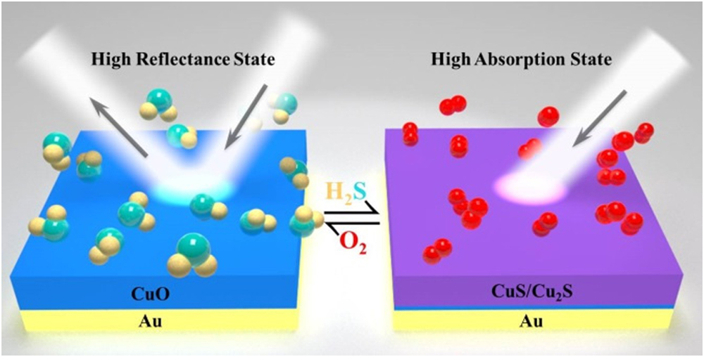
    Fig. 1. Schematic of the lithography-free, wide-angle, and dynamically reconfigurable subwavelength optical device, composed of hydrogen sulfide responsive CuO thin films on an optical thick gold (Au) substrate by utilizing the reversible chemical conversion of CuO to sulfides (CuS/Cu2S) upon exposure to H2S contained air (O2). The optical responses (high reflectance state/high absorption state) of the optical device were reconfigurable upon hydrogen sulfide exposure through phase-transition from CuO to CuS/Cu2S.
    (a1)–(a5) Schematic of the fabrication process of the proposed reconfigurable subwavelength optical device nanostructure. Here, L.T. denotes low temperature annealing at 40°C, and H.T. denotes high temperature annealing at 400°C. Corresponding surface (b1)–(b5) and cross-sectional (c1)–(c5) SEM images of the fabricated sample. Scale bars are 200 nm. Corresponding copper (Cu) element (d1)–(d5) and sulfur (S) element (e1)–(e5) spectra were detected by high-resolution XPS.
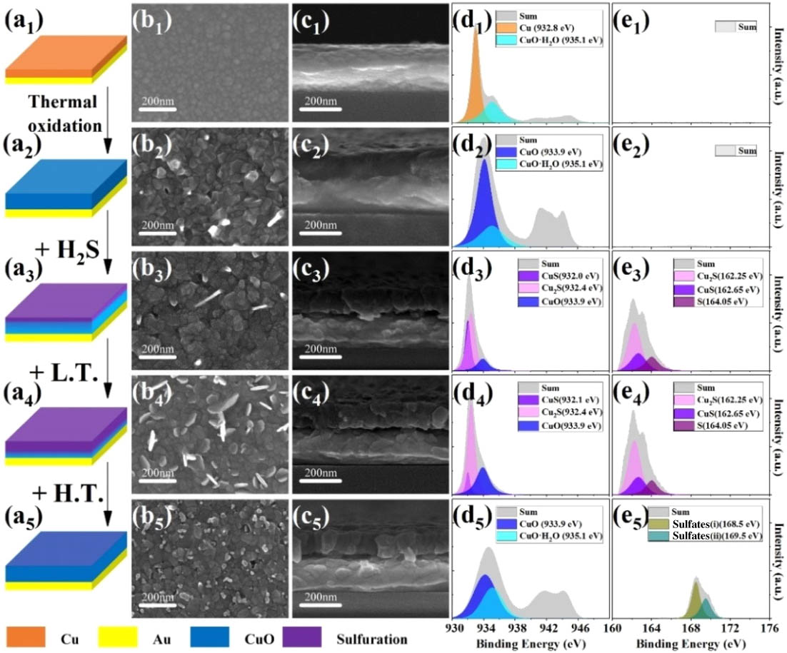
    Fig. 2. (a1)–(a5) Schematic of the fabrication process of the proposed reconfigurable subwavelength optical device nanostructure. Here, L.T. denotes low temperature annealing at 40°C, and H.T. denotes high temperature annealing at 400°C. Corresponding surface (b1)–(b5) and cross-sectional (c1)–(c5) SEM images of the fabricated sample. Scale bars are 200 nm. Corresponding copper (Cu) element (d1)–(d5) and sulfur (S) element (e1)–(e5) spectra were detected by high-resolution XPS.
    (a)–(d) Experimental realization of reconfigurable subwavelength optical device when the initial thickness of the top CuO layer d=35, 110, 150, and 180 nm, respectively. (e)–(h) Corresponding TMM calculated results of reflectance versus wavelength for the four cases. Both experimental and theoretical spectra are found to be in good accordance. State i: initial state as fabricated; state ii: fully reacting state; state iii: low temperature annealing state; state iv: high temperature annealing state.
    Fig. 3. (a)–(d) Experimental realization of reconfigurable subwavelength optical device when the initial thickness of the top CuO layer d=35, 110, 150, and 180 nm, respectively. (e)–(h) Corresponding TMM calculated results of reflectance versus wavelength for the four cases. Both experimental and theoretical spectra are found to be in good accordance. State i: initial state as fabricated; state ii: fully reacting state; state iii: low temperature annealing state; state iv: high temperature annealing state.
    Trajectory of sums of the calculated partially reflected waves for four different states studied in Fig. 3(g), with the initial thickness of the top CuO layer d=150 nm. Insets are the corresponding normalized electric field amplitudes.
    Fig. 4. Trajectory of sums of the calculated partially reflected waves for four different states studied in Fig. 3(g), with the initial thickness of the top CuO layer d=150  nm. Insets are the corresponding normalized electric field amplitudes.
    (a)–(c) Experimental and (d)–(f) calculated reflectance mapping spectra as a function of wavelengths and incident angles for TE, TM, and unpolarized light, respectively. Here, initial thickness of the top CuO layer d=150 nm upon exposure to 4% H2S in air at L.T. at 40°C.
    Fig. 5. (a)–(c) Experimental and (d)–(f) calculated reflectance mapping spectra as a function of wavelengths and incident angles for TE, TM, and unpolarized light, respectively. Here, initial thickness of the top CuO layer d=150  nm upon exposure to 4% H2S in air at L.T. at 40°C.
    Reflectance of the reconfigurable subwavelength optical device for different H2S volume fractions of (a) 1%, (b) 2%, (c) 3%, and (d) 4% in air. Our sensor exhibits largest relative intensity change up to 90% (magenta lines) at 1.79 μm upon exposure to 4% H2S in air. The increasing volume fractions lead to a pronounced relative intensity change of the reflectance spectrum.
    Fig. 6. Reflectance of the reconfigurable subwavelength optical device for different H2S volume fractions of (a) 1%, (b) 2%, (c) 3%, and (d) 4% in air. Our sensor exhibits largest relative intensity change up to 90% (magenta lines) at 1.79 μm upon exposure to 4% H2S in air. The increasing volume fractions lead to a pronounced relative intensity change of the reflectance spectrum.
    Retrieved refractive indices (n) and extinction coefficients (k) of (a) CuO and (b) CuS thin films.
    Fig. 7. Retrieved refractive indices (n) and extinction coefficients (k) of (a) CuO and (b) CuS thin films.
    Schematic illustration of light propagation in two subwavelength absorbing films on an optical opaque metallic reflector.
    Fig. 8. Schematic illustration of light propagation in two subwavelength absorbing films on an optical opaque metallic reflector.
    Repeatability and stability tests of the reflectance spectrum for four different thicknesses of top CuO film samples with (a) 35 nm, (b) 110 nm, (c) 150 nm, and (d) 180 nm, upon exposure to 1% (volume fraction) H2S in air.
    Fig. 9. Repeatability and stability tests of the reflectance spectrum for four different thicknesses of top CuO film samples with (a) 35 nm, (b) 110 nm, (c) 150 nm, and (d) 180 nm, upon exposure to 1% (volume fraction) H2S in air.
    Zhengji Wen, Jialiang Lu, Weiwei Yu, Hao Wu, Hao Xie, Xiaohang Pan, Qianqian Xu, Ziji Zhou, Chong Tan, Dongjie Zhou, Chang Liu, Yan Sun, Ning Dai, Jiaming Hao. Dynamically reconfigurable subwavelength optical device for hydrogen sulfide gas sensing[J]. Photonics Research, 2021, 9(10): 2060
    Download Citation