
Zhengji Wen, Jialiang Lu, Weiwei Yu, Hao Wu, Hao Xie, Xiaohang Pan, Qianqian Xu, Ziji Zhou, Chong Tan, Dongjie Zhou, Chang Liu, Yan Sun, Ning Dai, Jiaming Hao, "Dynamically reconfigurable subwavelength optical device for hydrogen sulfide gas sensing," Photonics Res. 9, 2060 (2021)
- Photonics Research
- Vol. 9, Issue 10, 2060 (2021)
Abstract
1. INTRODUCTION
In recent years, active modulation of light has become an important driving force for progress with many emerging concepts and applications [1–3]. Different from passive nanostructures that usually exhibit fixed responses and cannot be dynamically altered once being fabricated [4–7], the emerging active tuning methods combined with various functional materials bring excellent tunability to optical systems [8–11]. A plethora of tuning mechanisms including electrical [12,13], thermal [14,15], optical [16], and mechanical stretching [17] have been put forward for designing reconfigurable devices with versatile functionality, ultrathin features, and easiness for integration. Such tunable devices could be achieved by employing active materials that can have their properties changed through exposure to external stimuli, such as phase change materials [18–23], liquid crystals [24–27], transparent conductive oxides [28–30], and semiconductors [31,32], and have been realized for various frequency regions. However, mastering dynamic spectral control in the near-infrared (NIR) remains a challenging task, mainly ascribed to unattainable functional materials at high frequencies [20].
In this work, we experimentally demonstrate a novel paradigm of lithography-free, wide-angle, and reconfigurable subwavelength optical devices with high tunability in the NIR regions, based on a reversible nanochemistry approach [33–39]. Our proposed reconfigurable optical device basically consists of an ultrathin, highly absorbing dielectric layer [copper oxide (CuO)] deposited on an optical opaque metallic substrate [gold (Au)], as shown in Fig. 1. The optical responses (high reflectance state/high absorption state) of the optical device were reconfigurable upon hydrogen sulfide exposure. In our design, a chemically responsive CuO material is chosen, mainly due to two factors: (1) it is a highly absorbing medium at visible and NIR wavelength regimes, which would benefit producing strong optical asymmetric Fabry–Pérot (FP)-type interference effects [40,41]; (2) as a pure p-type metal oxide semiconductor, it has a strong chemical affinity to acidic hydrogen sulfide (
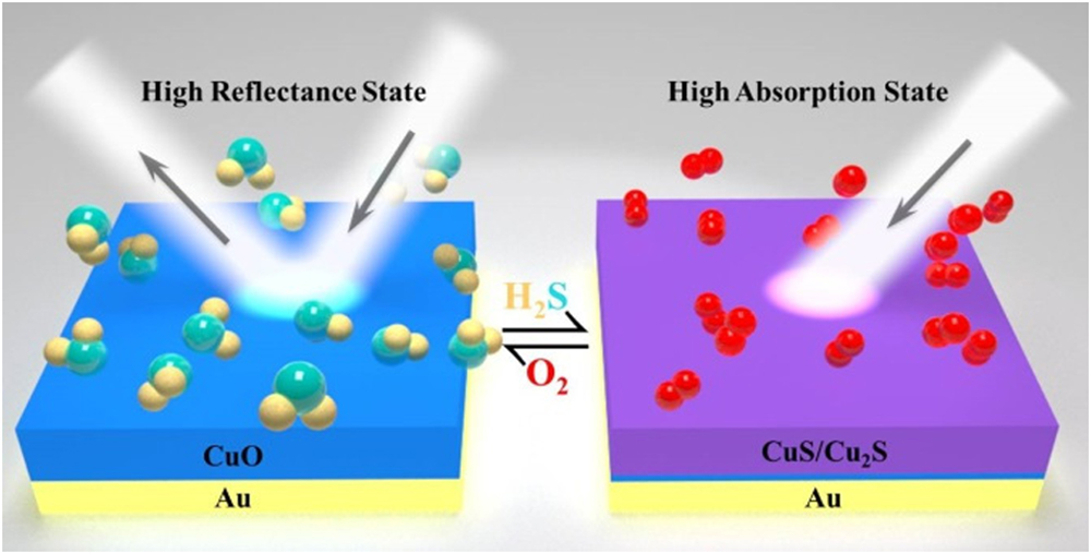
Figure 1.Schematic of the lithography-free, wide-angle, and dynamically reconfigurable subwavelength optical device, composed of hydrogen sulfide responsive CuO thin films on an optical thick gold (Au) substrate by utilizing the reversible chemical conversion of CuO to sulfides (
2. EXPERIMENT
A. Materials Preparation and Fabrication
Single-polished silicon (Si) substrates, each piece about
Sign up for Photonics Research TOC. Get the latest issue of Photonics Research delivered right to you!Sign up now
The whole fabrication procedure of the reconfigurable subwavelength optical device is schematically depicted in Figs. 2(a1)–2(a5). We first deposited a 200 nm thick Au film on a cleaned Si wafer by thermal evaporation (PZF-300, KYKY), serving as a mirror to eliminate light transmission. To prevent the Au film from falling off by the lattice mismatch between the Au film and Si wafer, a 5 nm titanium (Ti) as an adhesive layer was deposited on the Si wafer before depositing the Au layer. Then, five different thick copper (Cu) films (20, 40, 60, 80, and 100 nm) were sequentially deposited onto the Au film by a high vacuum double ion beam sputtering method (BAL-TEC, SCD 500). Next, the samples were placed on an LED constant temperature heating table (SET-217) in a muffle furnace for thermal oxidation annealing in air at 400°C for 2 h. In this process, the metallic Cu films were fully oxidized to CuO films with corresponding thicknesses of
![]()
Figure 2.(a1)–(a5) Schematic of the fabrication process of the proposed reconfigurable subwavelength optical device nanostructure. Here, L.T. denotes low temperature annealing at 40°C, and H.T. denotes high temperature annealing at 400°C. Corresponding surface (b1)–(b5) and cross-sectional (c1)–(c5) SEM images of the fabricated sample. Scale bars are 200 nm. Corresponding copper (Cu) element (d1)–(d5) and sulfur (S) element (e1)–(e5) spectra were detected by high-resolution XPS.
![]()
Figure 3.(a)–(d) Experimental realization of reconfigurable subwavelength optical device when the initial thickness of the top CuO layer
![]()
Figure 4.Trajectory of sums of the calculated partially reflected waves for four different states studied in Fig.
![]()
Figure 5.(a)–(c) Experimental and (d)–(f) calculated reflectance mapping spectra as a function of wavelengths and incident angles for TE, TM, and unpolarized light, respectively. Here, initial thickness of the top CuO layer
The prepared samples were then placed in a 5 mL centrifuge tube, followed by injecting
B. Characterization and Measurements
Morphologies of the corresponding fabricated samples were characterized by a scanning electron microscope (SEM, FEI Sirion 200) on high-resolution mode with 200 nm scale bars. Figures 2(b1)–2(b5) and 2(c1)–(c5) show the surface/cross section SEM images of a fabricated sample before annealing (with 80 nm Cu film) and after annealing (with 150 nm CuO film), respectively. Figure 2(b1) shows that the quality of the forming film was fairly good and thus the surface was smooth. A sharp interface between Si and Au is observed in Fig. 2(c1), while there is no distinct boundary between Au and Cu. As shown in Fig. 2(b2), granular crystallization on the surface appears, attributed to the recrystallization of Cu during the thermal oxidation process, resulting in a rough CuO surface. The thickness of the top layer is increased by a factor of
To investigate the elements of the corresponding nanolayer film, X-ray photoelectron spectroscopy (XPS, Thermo ESCALAB 250X) measurements using monochromated Al
The experimental visible and NIR reflection spectra were recorded using a UV-VIS-NIR spectrophotometer (PerkinElmer Lamda 950). The angle-resolved infrared reflectance (absorbance) spectrum measurements were characterized using a Fourier transform infrared (FTIR, Bruker IFS 66 v/S) spectrometer for both TE- and TM-polarized light, equipped with a reflection module allowing for angles ranging from 13° to 80°. The measured reflectance spectra were normalized with respect to an Au mirror, and unpolarized reflectance was obtained by
3. RESULTS AND DISCUSSION
Figures 3(a)–3(d) display the experimental reflectance spectra for four different thicknesses of CuO thin films (
Reactions could happen simultaneously including chemical Eqs. (1) and (2) at room temperature. Low temperature annealing (40°C) of the films was then performed for further optimization, and the obtained results are shown in Fig. 3 marked as state iii (olive lines). Slight changes in the reflectance are observed, which can be attributed to the redistribution of the above two chemical reactions.
After high temperature annealing at 400°C (state iv, red lines), the reflectance nearly returns to the initial states (state i, black lines), mainly ascribed to the chemical conversion [42]
The corresponding theoretical reflectance spectra calculated by transfer matrix methods (TMMs) [46,47] are presented in Figs. 3(e)–3(h). Both experimental and theoretical data are found to be in good agreement, and show that the resonances can easily be tuned by adjusting the initial thickness of CuO films. The slight difference between experimental and calculated optical reflectance spectra mainly results from random thickness fluctuations and diffusive intermixing at the interfaces [48–52]. It is noted that as the initial thickness of CuO thin films was taken as 150 nm [Fig. 3(c)], large tunability results can be achieved within the wavelength region of our interest; this is mainly due to the fact that the critical coupling conditions between the absorptive and radiative losses of this structure are matched [53–55].
We performed partially reflected wave calculations based on a multiple scattering model to further investigate the optical properties of our proposed subwavelength optical devices [40]. Figure 4 shows complex phasor diagrams of reflection coefficients for the structures at the four different states seen in Fig. 3(g) with the initial thickness of the top CuO layer
Here,
We know that when light is reflected from a highly absorbing layer on a metallic substrate, the phase of a complex reflection coefficient can deviate significantly from
To provide further theoretical insight, electric field distributions inside the structure under the same conditions are investigated. As shown in the insets of Fig. 4, the corresponding normalized electric field amplitudes are enhanced inside the absorbing film layer, which show excellent agreement with the partially reflected wave calculations. These calculations not only confirm that the asymmetric FP resonances indeed occur in these ultrathin films, but also verify the feasibility of our optical device, which possesses unique advantages for the design of a specific functional gas sensor. All of these results demonstrate that the feature of our subwavelength optical device indeed exhibits good reconfigurable properties, and highlight its potential application as a highly sensitive
Angular responses of the resonance effects were also investigated. Figures 5(a)–5(c) show the measured reflectance of the sample (here, 150 nm CuO film on state iii was chosen) as a function of wavelength and incident angle for TE, TM, and unpolarized light, respectively. The corresponding calculated reflectance spectra based on TMM are presented in Figs. 5(d)–5(f), and show good agreement with experimental results. Good angle-robust resonance performances are observed for all polarizations. This phenomenon is ascribed to the ultrathin feature of the structure with little phase accumulation; therefore, our optical devices are indeed very robust with respect to incident angles and polarizations. This unique angular-insensitivity characteristic of our subwavelength optical device indicates that it will have great potential in wide-angle sensing applications.
Finally,
![]()
Figure 6.Reflectance of the reconfigurable subwavelength optical device for different
4. CONCLUSION
To summarize, we demonstrated a reconfigurable subwavelength optical device with simple planar thin-film stacks, which is composed of an ultrathin, highly absorbing CuO thin film on an optically thick gold substrate based on the reversible chemical conversion of CuO to sulfides. Experimental results show that our optical device exhibits a relative reflection amplitude modulation depth as high as 90% at the wavelength of 1.79 μm. Theoretical analyses show that the working mechanism of the wide-angle and highly tunable optical device is due to strong optical asymmetric FP thin-film resonance interference combined with reversible chemical conversion, and is found to be in good agreement with experimental results. Furthermore, to illustrate the versatility of the optical device,
APPENDIX A: ELLIPSOMETRY DATA ANALYSES
We certify that the reconfigurable optical device is achieved by utilizing the reversible chemical conversion of CuO to CuS upon exposure to
![]()
Figure 7.Retrieved refractive indices (
APPENDIX B: PARTIALLY REFLECTED WAVE CALCULATIONS
For a theoretical description of the physical mechanisms to achieve perfect absorption, as shown in Fig.
![]()
Figure 8.Schematic illustration of light propagation in two subwavelength absorbing films on an optical opaque metallic reflector.
Here,
On the other hand, the reflection coefficient for such a system can be obtained by the coherent sum of the partially reflection waves, namely [
Here,
Finally, the total reflectance can thus be obtained by
As shown in Fig.
APPENDIX C: REPEATABILITY AND STABILITY TESTS
To verify the robustness of the experimental gas sensing tests, low volume fractions down to 1%
![]()
Figure 9.Repeatability and stability tests of the reflectance spectrum for four different thicknesses of top CuO film samples with (a) 35 nm, (b) 110 nm, (c) 150 nm, and (d) 180 nm, upon exposure to 1% (volume fraction)
References
[1] O. Hess, J. B. Pendry, S. A. Maier, R. F. Oulton, J. M. Hamm, K. L. Tsakmakidis. Active nanoplasmonic metamaterials. Nat. Mater., 11, 573-584(2012).
[2] J. Y. Ou, E. Plum, J. Zhang, N. I. Zheludev. An electromechanically reconfigurable plasmonic metamaterial operating in the near-infrared. Nat. Nanotechnol., 8, 252-255(2013).
[3] Q. He, S. Sun, L. Zhou. Tunable/reconfigurable metasurfaces: physics and applications. Research, 2019, 1849272(2019).
[4] X. Liu, Z. Li, Z. Wen, M. Wu, J. Lu, X. Chen, X. Zhao, T. Wang, R. Ji, Y. Zhang, L. Sun, B. Zhang, H. Xu, J. Zhou, J. Hao, S. Wang, X. Chen, N. Dai, W. Lu, X. Shen. Large-area, lithography-free, narrow-band and highly directional thermal emitter. Nanoscale, 11, 19742-19750(2019).
[5] J. Hao, J. Wang, X. Liu, W. J. Padilla, L. Zhou, M. Qiu. High performance optical absorber based on a plasmonic metamaterial. Appl. Phys. Lett., 96, 251104(2010).
[6] W. Zhao, Z. Wen, Q. Xu, Z. Zhou, S. Li, S. Fang, T. Chen, L. Sun, X. Wang, Y. Liu, Y. Sun, Y. W. Tan, N. Dai, J. Hao. Remarkable photoluminescence enhancement of CsPbBr3 perovskite quantum dots assisted by metallic thin films. Nanophotonics, 10, 2257-2264(2021).
[7] X. Ruan, W. Dai, W. Wang, C. Ou, Q. Xu, Z. Zhou, Z. Wen, C. Liu, J. Hao, Z. Guan, H. Xu. Ultrathin, broadband, omnidirectional, and polarization-independent infrared absorber using all-dielectric refractory materials. Nanophotonics, 10, 1683-1690(2021).
[8] L. Kang, R. P. Jenkins, D. H. Werner. Recent progress in active optical metasurfaces. Adv. Opt. Mater., 7, 1801813(2019).
[9] M. A. Mohammed, J. Melskens, R. Stabile, F. Pagliano, C. Li, W. M. M. Kessels, O. Raz. Metastable refractive index manipulation in hydrogenated amorphous silicon for reconfigurable photonics. Adv. Opt. Mater., 8, 1901680(2020).
[10] A. Nemati, Q. Wang, M. Hong, J. Teng. Tunable and reconfigurable metasurfaces and metadevices. Opto-Electron. Adv., 1, 18000901(2018).
[11] I. Kim, J. Yun, T. Badloe, H. Park, T. Seo, Y. Yang, J. Kim, Y. Chung, J. Rho. Structural color switching with a doped indium-gallium-zinc-oxide semiconductor. Photon. Res., 8, 1381-1387(2020).
[12] J. Y. Ou, E. Plum, L. Jiang, N. I. Zheludev. Reconfigurable photonic metamaterials. Nano Lett., 11, 2142-2144(2011).
[13] C. Meng, P. C. V. Thrane, F. Ding, J. Gjessing, M. Thomaschewski, C. Wu, C. Dirdal, S. I. Bozhevolnyi. Dynamic piezoelectric MEMS-based optical metasurfaces. Sci. Adv., 7, eabg5639(2021).
[14] R. Singh, A. K. Azad, Q. X. Jia, A. J. Taylor, H.-T. Chen. Thermal tunability in terahertz metamaterials fabricated on strontium titanate single-crystal substrates. Opt. Lett., 36, 1230-1232(2011).
[15] L. Lei, F. Lou, K. Tao, H. Huang, X. Cheng, P. Xu. Tunable and scalable broadband metamaterial absorber involving VO2-based phase transition. Photon. Res., 7, 734-741(2019).
[16] Y. Zhu, X. Hu, Y. Fu, H. Yang, Q. Gong. Ultralow-power and ultrafast all-optical tunable plasmon-induced transparency in metamaterials at optical communication range. Sci. Rep., 3, 2338(2013).
[17] H. S. Ee, R. Agarwal. Tunable metasurface and flat optical zoom lens on a stretchable substrate. Nano Lett., 16, 2818-2823(2016).
[18] S. G.-C. Carrillo, A. M. Alexeev, Y.-Y. Au, C. D. Wright. Reconfigurable phase-change meta-absorbers with on-demand quality factor control. Opt. Express, 26, 25567-25581(2018).
[19] N. Mou, X. Liu, T. Wei, H. Dong, Q. He, L. Zhou, Y. Zhang, L. Zhang, S. Sun. Large-scale, low-cost, broadband and tunable perfect optical absorber based on phase-change material. Nanoscale, 12, 5374-5379(2020).
[20] Z. Zhu, P. G. Evans, R. F. Haglund, J. G. Valentine. Dynamically reconfigurable metadevice employing nanostructured phase-change materials. Nano Lett., 17, 4881-4885(2017).
[21] Y. Wang, P. Landreman, D. Schoen, K. Okabe, A. Marshall, U. Celano, H. S. P. Wong, J. Park, M. L. Brongersma. Electrical tuning of phase-change antennas and metasurfaces. Nat. Nanotechnol., 16, 667-672(2021).
[22] F. Ding, Y. Yang, S. I. Bozhevolnyi. Dynamic metasurfaces using phase-change chalcogenides. Adv. Opt. Mater., 7, 1801709(2019).
[23] C. Ruiz de Galarreta, S. G. C. Carrillo, Y. Y. Au, E. Gemo, L. Trimby, J. Shields, E. Humphreys, J. Faneca, L. Cai, A. Baldycheva, J. Bertolotti, C. D. Wright. Tunable optical metasurfaces enabled by chalcogenide phase-change materials: from the visible to the THz. J. Opt., 22, 114001(2020).
[24] D. Shrekenhamer, W. C. Chen, W. J. Padilla. Liquid crystal tunable metamaterial absorber. Phys. Rev. Lett., 110, 177403(2013).
[25] S. Q. Li, X. Xu, R. M. Veetil, V. Valuckas, R. Paniagua-Domínguez, A. I. Kuznetsov. Phase-only transmissive spatial light modulator based on tunable dielectric metasurface. Science, 364, 1087-1090(2019).
[26] J. Li, P. Yu, S. Zhang, N. Liu. Electrically-controlled digital metasurface device for light projection displays. Nat. Commun., 11, 3574(2020).
[27] I. Kim, W. S. Kim, K. Kim, M. A. Ansari, M. Q. Mehmood, T. Badloe, Y. Kim, J. Gwak, H. Lee, Y. K. Kim, J. Rho. Holographic metasurface gas sensors for instantaneous visual alarms. Sci. Adv., 7, eabe9943(2021).
[28] J. Park, J. H. Kang, S. J. Kim, X. Liu, M. L. Brongersma. Dynamic reflection phase and polarization control in metasurfaces. Nano Lett., 17, 407-413(2017).
[29] Y. Lee, J. Yun, S. J. Kim, M. Seo, S. In, H. D. Jeong, S. Y. Lee, N. Park, T. D. Chung, B. Lee. High-speed transmission control in gate-tunable metasurfaces using hybrid plasmonic waveguide mode. Adv. Opt. Mater., 8, 2001256(2020).
[30] J. Park, B. G. Jeong, S. Il Kim, D. Lee, J. Kim, C. Shin, C. B. Lee, T. Otsuka, J. Kyoung, S. Kim, K. Y. Yang, Y. Y. Park, J. Lee, I. Hwang, J. Jang, S. H. Song, M. L. Brongersma, K. Ha, S. W. Hwang, H. Choo, B. L. Choi. All-solid-state spatial light modulator with independent phase and amplitude control for three-dimensional LiDAR applications. Nat. Nanotechnol., 16, 69-76(2021).
[31] H. T. Chen, W. J. Padilla, J. M. O. Zide, A. C. Gossard, A. J. Taylor, R. D. Averitt. Active terahertz metamaterial devices. Nature, 444, 597-600(2006).
[32] P. C. Wu, R. A. Pala, G. K. Shirmanesh, W. H. Cheng, R. Sokhoyan, M. Grajower, M. Z. Alam, D. Lee, H. A. Atwater. Dynamic beam steering with all-dielectric electro-optic III–V multiple-quantum-well metasurfaces. Nat. Commun., 10, 3654(2019).
[33] A. Tittl, P. Mai, R. Taubert, D. Dregely, N. Liu, H. Giessen. Palladium-based plasmonic perfect absorber in the visible wavelength range and its application to hydrogen sensing. Nano Lett., 11, 4366-4369(2011).
[34] F. Sterl, N. Strohfeldt, R. Walter, R. Griessen, A. Tittl, H. Giessen. Magnesium as novel material for active plasmonics in the visible wavelength range. Nano Lett., 15, 7949-7955(2015).
[35] M. Li, D. Liu, H. Cheng, L. Peng, M. Zu. Manipulating metals for adaptive thermal camouflage. Sci. Adv., 6, eaba3494(2020).
[36] J. Karst, M. Hentschel, F. Sterl, H. Giessen. Liquid hydrogenation of plasmonic nanoantennas via alcohol deprotonation. ACS Photon., 8, 1810-1816(2021).
[37] Y. Jin, L. Zhou, J. Liang, J. Zhu. Electrochemically driven dynamic plasmonics. Adv. Photon., 3, 044002(2021).
[38] A. Böhme, F. Sterl, E. Kath, M. Ubl, V. Manninen, H. Giessen. Electrochemistry on inverse copper nanoantennas: active plasmonic devices with extraordinarily large resonance shift. ACS Photon., 6, 1863-1868(2019).
[39] Y. Lee, J. Yun, M. Seo, S. J. Kim, J. Oh, C. M. Kang, H. J. Sun, T. D. Chung, B. Lee. Full-color-tunable nanophotonic device using electrochromic tungsten trioxide thin film. Nano Lett., 20, 6084-6090(2020).
[40] H. Pan, Z. Wen, Z. Tang, G. Xu, X. Pan, Q. Xu, Y. Lu, H. Xu, Y. Sun, N. Dai, J. Hao. Wide gamut, angle-insensitive structural colors based on deep-subwavelength bilayer media. Nanophotonics, 9, 3385-3392(2020).
[41] M. A. Kats, R. Blanchard, P. Genevet, F. Capasso. Nanometre optical coatings based on strong interference effects in highly absorbing media. Nat. Mater., 12, 20-24(2013).
[42] A. Paul, C. Weinberger, M. Tiemann, T. Wagner. Copper oxide/silica nanocomposites for selective and stable H2S gas detection. ACS Appl. Nano Mater., 2, 3335-3338(2019).
[43] S. K. Ganapathi, M. Kaur, R. Singh, V. I. Singh, A. K. Debnath, K. P. Muthe, S. C. Gadkari. Anomalous sensing response of NiO nanoparticulate films toward H2S. ACS Appl. Nano Mater., 2, 6726-6737(2019).
[44] K. Khaliji, S. R. Biswas, H. Hu, X. Yang, Q. Dai, S. H. Oh, P. Avouris, T. Low. Plasmonic gas sensing with graphene nanoribbons. Phys. Rev. Appl., 13, 011002(2020).
[45] E. D. Palik. Handbook of Optical Constants of Solids(1985).
[46] P. Yeh. Optical Wave in Layered Media(1988).
[47] Z. Wen, H. Xu, W. Zhao, Z. Zhou, X. Li, S. Li, J. Zhou, Y. Sun, N. Dai, J. Hao. Nonlocal effective-medium theory for periodic multilayered metamaterials. J. Opt., 23, 065103(2021).
[48] R. Ravi, A. Paul. Diffusion mechanism in the gold-copper system. J. Mater. Sci. Mater. Electron., 23, 2152-2156(2012).
[49] S. Liu, Z. Sun, Q. Liu, L. Wu, Y. Huang, T. Yao, J. Zhang, T. Hu, M. Ge, F. Hu, Z. Xie, G. Pan, S. Wei. Unidirectional thermal diffusion in bimetallic Cu-Au nanoparticles. ACS Nano, 8, 1886-1892(2014).
[50] L. Lu, W. Dong, J. K. Behera, L. Chew, R. E. Simpson. Inter-diffusion of plasmonic metals and phase change materials. J. Mater. Sci., 54, 2814-2823(2019).
[51] A. B. Martin, R. D. Johnson, F. Asaro. Diffusion of gold into copper. J. Appl. Phys., 25, 364-369(1954).
[52] J. Shields, C. R. de Galarreta, J. Bertolotti, C. D. Wright. Enhanced performance and diffusion robustness of phase-change metasurfaces via a hybrid dielectric/plasmonic approach. Nanomaterials, 11, 525(2021).
[53] H. A. Haus. Waves and Fields in Optoelectronics(1984).
[54] S. Fan, W. Suh, J. D. Joannopoulos. Temporal coupled-mode theory for the Fano resonance in optical resonators. J. Opt. Soc. Am. A, 20, 569-572(2003).
[55] C. Qu, S. Ma, J. Hao, M. Qiu, X. Li, S. Xiao, Z. Miao, N. Dai, Q. He, S. Sun, L. Zhou. Tailor the functionalities of metasurfaces based on a complete phase diagram. Phys. Rev. Lett., 115, 235503(2015).
[56] B. H. Woo, I. C. Seo, E. Lee, S. Y. Kim, T. Y. Kim, S. C. Lim, H. Y. Jeong, C. K. Hwangbo, Y. C. Jun. Dispersion control of excitonic thin films for tailored superabsorption in the visible region. ACS Photon., 4, 1138-1145(2017).
[57] M. A. Kats, D. Sharma, J. Lin, P. Genevet, R. Blanchard, Z. Yang, M. M. Qazilbash, D. N. Basov, S. Ramanathan, F. Capasso. Ultra-thin perfect absorber employing a tunable phase change material. Appl. Phys. Lett., 101, 221101(2012).
[58] C. U. Hail, A. K. U. Michel, D. Poulikakos, H. Eghlidi. Optical metasurfaces: evolving from passive to adaptive. Adv. Opt. Mater., 7, 1801786(2019).


Set citation alerts for the article
Please enter your email address

© Copyright 2018-2021 | Chinese Laser Press. All Rights Reserved 沪ICP备15018463号-20