
Mengzhen Hao, Fengping Yan, Wei Wang, Xuemei Du, Hong Huo. Metamaterial-Based Terahertz Polarization-Insensitive Broadband Absorber[J]. Chinese Journal of Lasers, 2019, 46(12): 1214002
- Chinese Journal of Lasers
- Vol. 46, Issue 12, 1214002 (2019)
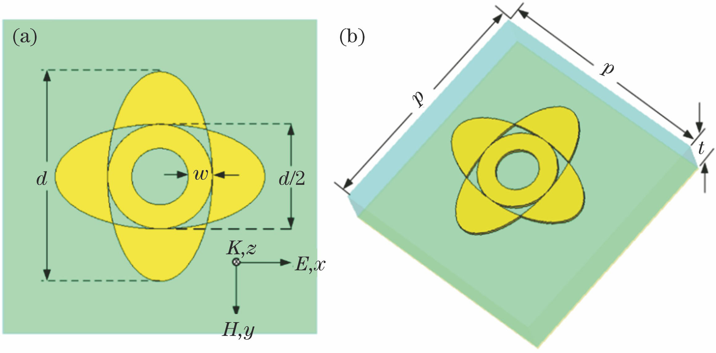
Fig. 1. Diagram of single peak absorber structure
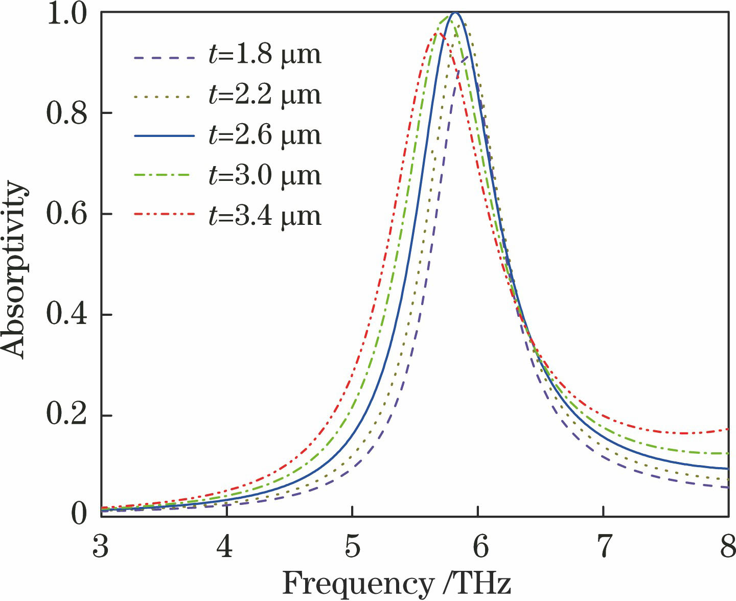
Fig. 2. Absorption spectra corresponding to different t when d=15 μm and w=1.6 μm
Fig. 3. Absorption spectra corresponding to different w when d=15 μm and t=2.6 μm
Fig. 4. Absorption spectra corresponding to different d when w=1.6 μm and t=2.6 μm
Fig. 5. Simulation results of surface current and z component of electric field intensity. (a) Surface current in surface metamaterial metal layer; (b) current in grounding metal layer; (c) z component of electric field intensity in surface metamaterial metal layer; (d) z component of electric field in grounding metal layer
Fig. 6. Diagram of three-layer wideband absorber
Fig. 7. Absorption spectrum of three-layer wideband absorber
Fig. 8. Diagram of two-layer wideband absorber
Fig. 9. Absorption spectrum of two-layer wideband absorber
Fig. 10. Electric field intensity distributions of two-layer absorber at two resonant frequencies
Fig. 11. Electric field intensity distributions of three-layer absorber at resonant frequencies
Fig. 12. Absorption spectra corresponding to different phase angles
Fig. 13. Absorption spectra corresponding to each incident angle under different polarization. (a) TE polarization; (b) TM polarization
|
Table 1. Structural and geometric parameters of three-layer wideband absorber
|
Table 2. Structural and geometric parameters of two-layer wideband absorber

Set citation alerts for the article
Please enter your email address
© Copyright 2018-2021 | Chinese Laser Press. All Rights Reserved 沪ICP备15018463号-20