
Xiao-Hui XIE, Chun LIN, Lu CHEN, Yu ZHAO, Jing ZHANG, Li HE. The passivation effects of CdTe deposited by MBE in MW HgCdTe photodiodes[J]. Journal of Infrared and Millimeter Waves, 2022, 41(2): 413
- Journal of Infrared and Millimeter Waves
- Vol. 41, Issue 2, 413 (2022)
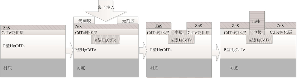
Fig. 1. Flow-process diagram of HgCdTe photodiodes passivated by the CdTe in-suit
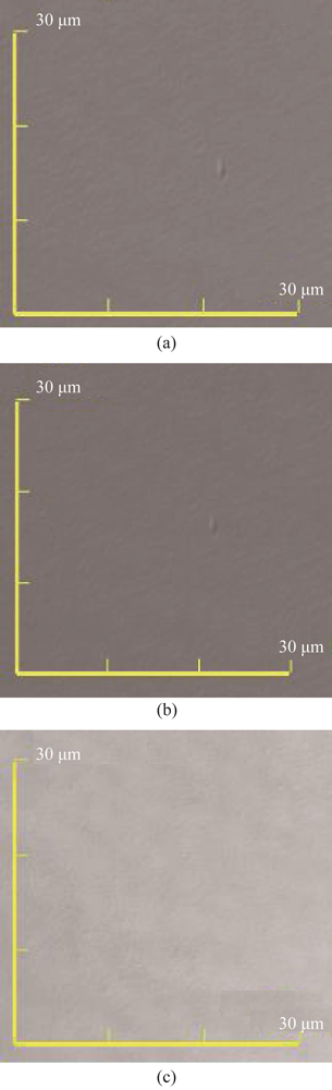
Fig. 2. Topography images of CdTe or HgCdTe using laser scanning confocal microscopy(a)CdTe deposited by MBE,(b)HgCdTe after etching CdTe in-suit, and(c)HgCdTe after etching top layer HgCdTe
Fig. 3. AFM topography images of CdTe or HgCdTe(a)CdTe deposited by MBE,(b)HgCdTe after etching CdTe in-suit, and(c)CdTe deposited by E-beam evaporation
Fig. 4. SEM top view images of CdTe or HgCdTe surface
Fig. 5. Cross-sectional SEM images of the CdTe and HgCdTe interface(a)cross-sectional images of CdTe deposited by MBE, and(b)cross-sectional images of CdTe deposited by E-beam evaporation
Fig. 6. I-V and R-V characteristics of HgCdTe photodiodes with different passivation layers(a)photodiodes passivated by CdTe in-suit,(b)photodiodes passivated by CdTe/ZnS,(c)photodiodes passivated by CdTe in-suit with annealing after implant, and(d)photodiodes passivated by CdTe/ZnS with annealing after implant

Set citation alerts for the article
Please enter your email address
© Copyright 2018-2021 | Chinese Laser Press. All Rights Reserved 沪ICP备15018463号-20