• Photonics Research
  • Vol. 6, Issue 3, 220 (2018)
Wenjun Liu1、2、†, Ya-Nan Zhu3、†, Mengli Liu1, Bo Wen3, Shaobo Fang2, Hao Teng2, Ming Lei1、5, Li-Min Liu3、4、6, and Zhiyi Wei2、*
Author Affiliations
  • 1State Key Laboratory of Information Photonics and Optical Communications, School of Science, Beijing University of Posts and Telecommunications, Beijing 100876, China
  • 2Beijing National Laboratory for Condensed Matter Physics, Institute of Physics, Chinese Academy of Sciences, Beijing 100190, China
  • 3Beijing Computational Science Research Center, Beijing 100193, China
  • 4School of Physics and Nuclear Energy Engineering, Beihang University, Beijing 100083, China
  • 5e-mail: mlei@bupt.edu.cn
  • 6e-mail: limin.liu@csrc.ac.cn
  • show less
    DOI: 10.1364/PRJ.6.000220 Cite this Article Set citation alerts
    Wenjun Liu, Ya-Nan Zhu, Mengli Liu, Bo Wen, Shaobo Fang, Hao Teng, Ming Lei, Li-Min Liu, Zhiyi Wei. Optical properties and applications for MoS2-Sb2Te3-MoS2 heterostructure materials[J]. Photonics Research, 2018, 6(3): 220 Copy Citation Text show less
    State-of-the-art SA devices using the MoS2-Sb2Te3-MoS2 heterostructure. (a) Schematic of macrostructure and (b) surface structure of the fabricated MoS2-Sb2Te3-MoS2 heterostructure SA. Sb2Te3 (7 nm thickness) is in the middle of MoS2 (8 nm thickness). The gold film with 117 nm thickness is deposited on the polished fused silica substrate as a broadband reflection mirror. (c) SEM image of the surface of deposited MoS2-Sb2Te3-MoS2 heterostructure film. (d) SEM image of the film thickness.
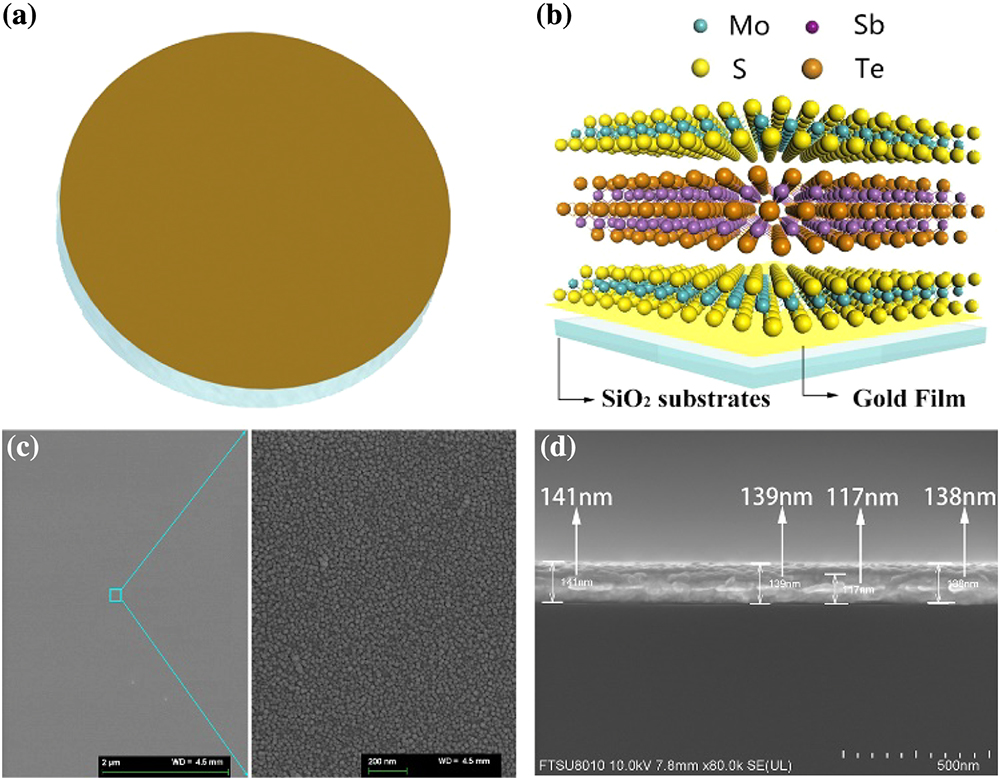
    Fig. 1. State-of-the-art SA devices using the MoS2-Sb2Te3-MoS2 heterostructure. (a) Schematic of macrostructure and (b) surface structure of the fabricated MoS2-Sb2Te3-MoS2 heterostructure SA. Sb2Te3 (7 nm thickness) is in the middle of MoS2 (8 nm thickness). The gold film with 117 nm thickness is deposited on the polished fused silica substrate as a broadband reflection mirror. (c) SEM image of the surface of deposited MoS2-Sb2Te3-MoS2 heterostructure film. (d) SEM image of the film thickness.
    Atomic and electronic structures of the MoS2-Sb2Te3-MoS2 heterostructure. (a) Side and (b) top views of the MoS2-Sb2Te3-MoS2 heterostructure. In (b), the detailed matching pattern of the (7×7)/(2×2)MoS2-Sb2Te3-MoS2 heterostructure is shown. The (7×7)MoS2 supercell is highlighted with yellow color, and the (2×2)Sb2Te supercell is denoted by the blue area. (c) Unfolding band structure of the MoS2-Sb2Te3-MoS2 heterostructure. Here, the Fermi level is defined as zero. (d) Band alignment of the MoS2-Sb2Te3-MoS2 heterostructure. The corresponding energy levels of pure MoS2 and Sb2Te3 slabs are shown in both sides.
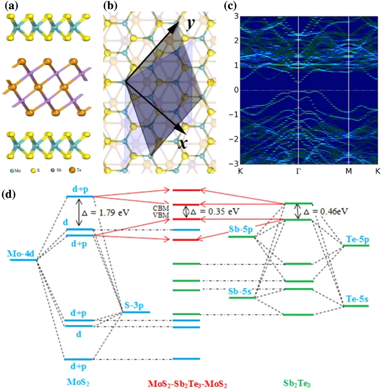
    Fig. 2. Atomic and electronic structures of the MoS2-Sb2Te3-MoS2 heterostructure. (a) Side and (b) top views of the MoS2-Sb2Te3-MoS2 heterostructure. In (b), the detailed matching pattern of the (7×7)/(2×2)MoS2-Sb2Te3-MoS2 heterostructure is shown. The (7×7)MoS2 supercell is highlighted with yellow color, and the (2×2)Sb2Te supercell is denoted by the blue area. (c) Unfolding band structure of the MoS2-Sb2Te3-MoS2 heterostructure. Here, the Fermi level is defined as zero. (d) Band alignment of the MoS2-Sb2Te3-MoS2 heterostructure. The corresponding energy levels of pure MoS2 and Sb2Te3 slabs are shown in both sides.
    Standard two-arm transmission setup. The SAM is the MoS2-Sb2Te3-MoS2 heterostructure SA mirror.
    Fig. 3. Standard two-arm transmission setup. The SAM is the MoS2-Sb2Te3-MoS2 heterostructure SA mirror.
    Characterization of the MoS2-Sb2Te3-MoS2 heterostructure SA mirror. (a) The modulation depth is 64.17%. (b) Raman spectrum of the MoS2-Sb2Te3-MoS2 heterostructure. (c), (d) Threshold damage condition of the MoS2-Sb2Te3-MoS2 heterostructure film at 12 mW.
    Fig. 4. Characterization of the MoS2-Sb2Te3-MoS2 heterostructure SA mirror. (a) The modulation depth is 64.17%. (b) Raman spectrum of the MoS2-Sb2Te3-MoS2 heterostructure. (c), (d) Threshold damage condition of the MoS2-Sb2Te3-MoS2 heterostructure film at 12 mW.
    Configuration of the mode-locked EDF laser. WDM, wavelength-division multiplexer; LD, laser diode; SMF, single-mode fiber; EDF, erbium-doped fiber; OC, optical coupler; PC, polarization controller; PI-ISO, polarization-independent isolator; SAM, MoS2-Sb2Te3-MoS2 heterostructure SA mirror.
    Fig. 5. Configuration of the mode-locked EDF laser. WDM, wavelength-division multiplexer; LD, laser diode; SMF, single-mode fiber; EDF, erbium-doped fiber; OC, optical coupler; PC, polarization controller; PI-ISO, polarization-independent isolator; SAM, MoS2-Sb2Te3-MoS2 heterostructure SA mirror.
    Typical Q-switching characteristics. (a) Q-switched pulse trains. (b) Optical spectrum. (c) Q-switched pulse duration at 600 mW pump power. (d) RF spectrum at the fundamental frequency and wideband RF spectrum (inset).
    Fig. 6. Typical Q-switching characteristics. (a) Q-switched pulse trains. (b) Optical spectrum. (c) Q-switched pulse duration at 600 mW pump power. (d) RF spectrum at the fundamental frequency and wideband RF spectrum (inset).
    (a) Pulse duration and repetition rate versus incident pump power. (b) Average output power and single pulse energy versus incident pump power.
    Fig. 7. (a) Pulse duration and repetition rate versus incident pump power. (b) Average output power and single pulse energy versus incident pump power.
    Experimental results of fiber laser with mode-locked states. (a) Optical spectrum. (b) Pulse duration. (c) RF spectrum. (d) Phase noise.
    Fig. 8. Experimental results of fiber laser with mode-locked states. (a) Optical spectrum. (b) Pulse duration. (c) RF spectrum. (d) Phase noise.
      Effective Mass (m0)Carrier Mobility (cm2·V1·s1)
    UnitsCarrier Typemx*my*μxμy
    MoS2e0.7740.47823.8794.04
    h3.1950.5508.5451.76
    Sb2Te3e0.2910.1570.75×1041.91×104
    h0.2840.0760.69×1042.12×104
    MoS2-Sb2Te3-MoS2e0.4050.3151560.978474.63
    h0.4230.620798.871447.54
    Graphene-Sb2Te3-graphenee7.7629.86013.505.96
    h1.5531.656149.23357.62
    Table 1. Effective Mass (m0) and Carrier Mobility (μ) of Monolayer and Heterostructure Materialsa
      Carrier Concentration (m2)
    UnitsBandgap (eV)nixniy
    MoS21.7913143.8
    Sb2Te30.463.11×10121.58×1012
    MoS2-Sb2Te3-MoS20.355.13×10131.03×1014
    Graphene-Sb2Te3-graphene0.077.26×10161.13×1017
    Table 2. Intrinsic Carrier Concentration of Monolayer and Heterostructure Materialsa
    MaterialsPulse duration (fs)SNR (dB)Modulation depth (%)Power (mW)References
    Graphene-Bi2Te3 heterostructure180067.418.98[55]
    Graphene-Bi2Te3 heterostructure83760.712.63.07[58]
    Graphene-Bi2Te3189940<5023.282.53[59]
    MoS2/graphene nanocomposites367053.738.3<2.16[60]
    Graphene/MoS28306010.85.85[61]
    Graphene/WS21120629.64.74[62]
    MoS2-Sb2Te3-MoS22867364.1720This work
    Table 3. Comparison of Fiber Lasers Based on Different Heterostructure SAs
    Wenjun Liu, Ya-Nan Zhu, Mengli Liu, Bo Wen, Shaobo Fang, Hao Teng, Ming Lei, Li-Min Liu, Zhiyi Wei. Optical properties and applications for MoS2-Sb2Te3-MoS2 heterostructure materials[J]. Photonics Research, 2018, 6(3): 220
    Download Citation