Abstract
Two-dimensional (2D) materials with potential applications in photonic and optoelectronic devices have attracted increasing attention due to their unique structures and captivating properties. However, generation of stable high-energy ultrashort pulses requires further boosting of these materials’ optical properties, such as higher damage threshold and larger modulation depth. Here we investigate a new type of heterostructure material with uniformity by employing the magnetron sputtering technique. Heterostructure materials are synthesized with van der Waals heterostructures consisting of and . The bandgap, carrier mobility, and carrier concentration of the heterostructure materials are calculated theoretically. By using these materials as saturable absorbers (SAs), applications in fiber lasers with -switching and mode-locking states are demonstrated experimentally. The modulation depth and damage threshold of SAs are measured to be 64.17% and , respectively. Both theoretical and experimental results indicate that heterostructure materials have large modulation depth, and can resist high power during the generation of ultrashort pulses. The heterostructure materials have the advantages of low cost, high reliability, and suitability for mass production, and provide a promising solution for the development of 2D-material-based devices with desirable electronic and optoelectronic properties.1. INTRODUCTION
Two-dimensional (2D) materials have exhibited great promise in microelectronics and optoelectronics since the discovery of graphene [1–9]. They possess special physical features, and can be used in the construction of various functional devices. Considered as one of the keys to modern technology, low-dimensional materials have been consistently reported and deeply investigated [10–20]. For example, carbon nanotubes (CNTs) and some 2D materials have been applied to the preparation of saturable absorption devices, photodetectors, and optical modulators [21–28].
As a saturable absorption material, CNTs are not sensitive to polarization, and have relatively high damage threshold and environmental stability. However, their scattering loss needs to be further reduced [29–31]. Graphene, which is cheap and convenient to prepare, also has a high damage threshold and ultra-fast recovery time [2–4]. As a special zero-gap semiconductor, graphene nearly absorbs the light for each band, which makes it suitable as an ultra-wide-band saturable absorber (SA). However, the modulation depth and non-saturable loss should be optimized [32–35]. Topological insulators (TIs), the generic term for materials with topological electronic properties, have the advantages of excellent saturable absorption property, large optical modulation depth, and high third-order nonlinear refractive index. Their narrow bandgap enhances their ability to absorb the broadband spectrum, which has potential applications in ultrafast optics [36–38]. Nevertheless, their thermal damage threshold should be improved [36–38]. Transition metal dichalcogenides (TMDs) have been widely investigated in nonlinear optics after graphene [39–45]. To date, molybdenum disulfide (), tungsten disulphide (), and tungsten diselenide () have been proved to have ultrafast electron relaxation ability. TMDs can act as saturable absorption materials. They have higher damage threshold, but their nonlinear absorption properties remain to be enhanced [39–45]. Black phosphorus has direct bandgap, and the carrier mobility is high. Although its easy oxidation brings about a bit of difficulty for its direct application [46–49], there are plenty of methods to encapsulate and enhance its stability that have achieved satisfactory results [50,51]. In addition, some novel 2D materials have garnered substantial interest. For instance, few-layer antimonene and few-layer bismuthene have successfully realized mode-locking operation [52,53]; they inject new vitality into the study of ultrafast lasers.
In fact, saturable absorption materials are composed of a monolayer or multilayer of atoms arrayed in 2D space or quasi-2D space with a certain thickness. They can be modularized, and then stacked together without lattice mismatch in traditional heterostructures [54–56]. Because different 2D materials have different bandgaps and energy band structures, they can be customized with different band structures according to various requirements [57–62]. Here, we provide heterostructure materials to produce SAs with higher damage threshold and larger modulation depth. The optical absorption intensity and modulation depth of the heterostructures can be greatly increased due to the greater modulation depth and stronger optical nonlinearity of . Compared with that of graphene, the damage threshold of is higher, and the modulation depth of single-layer is greater than that of graphene. Thus, will not introduce extra non-saturation losses on account of the increase in modulation depth. The damage threshold and modulation depth of SAs are measured to be and 64.17%, respectively, in experiment. The fabricated heterostructure SAs are integrated into an erbium-doped fiber (EDF) laser to demonstrate the related optical properties through -switching and mode-locking operation. Both the theoretical and experimental results indicate that the heterostructure materials have excellent optical properties in photonic device applications.
Sign up for Photonics Research TOC. Get the latest issue of Photonics Research delivered right to you!Sign up now
2. RESULTS AND DISCUSSION
A. Heterostructure Material Characterizations
The magnetron sputtering technique is employed to fabricate the heterostructure SAs. The heterostructure materials were divided into three layers, and were composed of and . The structures of the fabricated SAs are presented in Figs. 1(a) and 1(b). The gold film, which serves as a highly reflective mirror, was grown on polished fused silica substrate 1 inch in diameter. The target (diameter 60 mm, thickness 5 mm, purity 99.99%), target (diameter 49 mm, thickness 3.5 mm, purity 99.99%), and gold target (diameter 50 mm, thickness 2.5 mm, purity 99.9%) were placed in the target chambers, and the pressure in the vacuum chamber was set to be during the process of film deposition. At first, the Au target was excited under direct current (DC) voltage for 5 min with the gold film thickness of 117 nm. Then the sputtered sulfur and molybdenum atoms were ejected out from the target and deposited on the gold film.
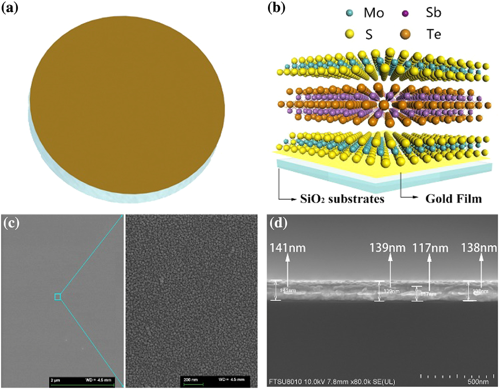
Figure 1.State-of-the-art SA devices using the heterostructure. (a) Schematic of macrostructure and (b) surface structure of the fabricated heterostructure SA. (7 nm thickness) is in the middle of (8 nm thickness). The gold film with 117 nm thickness is deposited on the polished fused silica substrate as a broadband reflection mirror. (c) SEM image of the surface of deposited heterostructure film. (d) SEM image of the film thickness.
The film, with thickness of 8 nm, was generated under 100 W radio frequency (RF) power for 1 min. Next, film with thickness of 7 nm was deposited on the film under 0.2 A DC current for 20 s. Finally, another film with the thickness of 8 nm was deposited on the film. The size and microstructure of the heterostructure materials were verified by scanning electron microscopy (SEM). In Figs. 1(c) and 1(d), the surface of the heterostructure materials on the left side of the graph is compact and robust, and the as-prepared samples are composed of some uniform-scale nanoparticles on the right side of the graph, which demonstrate 8 nm average size. It is generally agreed upon that small particle diameter leads to large active surface area. Therefore, it can be speculated that heterostructures have outstanding activity and superior conductivity. The overall thickness of the heterostructure in Fig. 1(d) is about 24 nm.
B. Bandgap
The heterostructure was modeled by a sandwich-layered structure in Fig. 2(a). To minimize the lattice mismatch between the and , a supercell of was used in Fig. 2(b), and the corresponding lattice mismatch is 2%. The corresponding unfolding band structure of the heterostructure was further examined with BandUP code [63,64]. The calculations were performed by density functional theory (DFT) implemented in the Vienna ab initio simulation package [65]. The interaction between core electrons and valence electrons was described with the projector augmented wave pseudopotential [66,67]. The valence electrons were expanded by plane wave functions with a 400 eV cutoff energy. The exchange-correlation energy was calculated by the use of the general gradient approximation of Perdew–Burke–Ernzerhof (PBE) [68]. Atomic spin-orbit coupling (SOC) was considered. The surface structures were modeled with a 20 Å vacuum separation between repeated slabs. To obtain the correct interlayer interaction in heterostructures, the van der Waals correction proposed by Grimme (DFT-D3) was enclosed [69]. By a mesh grid of k-points, the Brillouin zone was selected with the Gamma-centered Monkhorst–Pack scheme. The structure was relaxed until the change of the total energy was less than and the forces became less than 0.01 eV/Å.

Figure 2.Atomic and electronic structures of the heterostructure. (a) Side and (b) top views of the heterostructure. In (b), the detailed matching pattern of the heterostructure is shown. The supercell is highlighted with yellow color, and the supercell is denoted by the blue area. (c) Unfolding band structure of the heterostructure. Here, the Fermi level is defined as zero. (d) Band alignment of the heterostructure. The corresponding energy levels of pure and slabs are shown in both sides.
Bulk is a type of TI with a single Dirac cone. The calculated lattice constant of is 4.273 Å for a, and 29.975 Å for c using . These calculated constants agree well with the experimental values: 4.264 Å for a, and 30.458 Å for c [70]. The lattice constant of is 3.150 Å for a, and 11.99 Å for c.
The modulation depth of the heterostructure is related to the carrier relaxation time τ and carrier concentration . The relaxation time is associated with carrier mobility , and the in 2D materials can be calculated by the following equation [71,72]: where (or ) is the effective mass along the transport direction ( along the direction or along the direction, respectively), which can be extracted from the band structure calculation, and is the average effective mass defined by . represents the temperature taken as 300 K. is the deformation potential constant of the valence band maximum (VBM) for the hole and conduction band minimum (CBM) for electron, defined by , with the lattice compression or dilatation by a step of 0.5%. represents the effective 2D elastic moduli, which can be calculated by , where and are the total energies after deformation along the direction and at the equilibrium state, respectively. is the area of the 2D system at equilibrium. The intrinsic carrier concentration in 2D semiconductor materials can be computed through the following equation [73]: where is the energy bandgap. In Fig. 2(c), the bandgap of the is calculated to be 0.35 eV, slightly smaller than the bandgap of monolayer (0.46 eV). As shown in Table 1, the effective masses of holes along the and directions in the heterostructure are 0.620 and 0.423, respectively. The corresponding effective masses of electrons are 0.315 and 0.405, respectively. The effective masses of holes are slightly larger than those of electrons along the same direction. Meanwhile, the effective mass of either electron or hole is smaller than that of the monolayer , but a little larger than that of the monolayer .
| | | Effective Mass (m0) | Carrier Mobility (cm2 ·V−1· s−1) |
| Units | Carrier Type | mx* | my* | μx | μy |
| MoS2 | e | 0.774 | 0.478 | 23.87 | 94.04 |
| h | 3.195 | 0.550 | 8.54 | 51.76 |
| Sb2Te3 | e | 0.291 | 0.157 | 0.75×10⁴ | 1.91×10⁴ |
| h | 0.284 | 0.076 | 0.69×10⁴ | 2.12×10⁴ |
| MoS2-Sb2Te3-MoS2 | e | 0.405 | 0.315 | 1560.97 | 8474.63 |
| h | 0.423 | 0.620 | 798.87 | 1447.54 |
| Graphene-Sb2Te3-graphene | e | 7.762 | 9.860 | 13.50 | 5.96 |
| h | 1.553 | 1.656 | 149.23 | 357.62 |
Table 1. Effective Mass () and Carrier Mobility () of Monolayer and Heterostructure Materialsa
In Fig. 2(d), the bandgaps of the monolayers and are 1.79 and 0.46 eV, while that of the heterostructure is 0.35 eV. The main reason for this comes from the van der Waals interlayer coupling between antibonding hybrid orbitals of and hybrid orbitals of , which causes the rise in VBM and the reduction of CBM. Meanwhile, such weak coupling also affects the carrier mobility and concentration, as we discuss subsequently.
C. Carrier Mobility
The effective mass and carrier mobility of the heterostructure and monolayers and are shown in Table 1. The carrier mobility of the heterostructure is larger than that of the monolayer , but smaller than that of monolayer , which indicates that the relaxation time of is longer than that of monolayer but shorter than that of monolayer . The carrier mobility of is greatly affected by the relatively large effective mass compared with that of . In comparison with , grapheme--graphene shows a larger effective mass, and thus the graphene--graphene should have a shorter relaxation time than the . The relatively large carrier mobility of the heterostructure represents the long relaxation time of the structure, which is vital for applications in photonic devices.
D. Carrier Concentration
The intrinsic carrier concentration, which is closely related with the effective mass and bandgap, is further calculated. As shown in Table 2, the carrier concentration of the is 10–100 times larger than that of monolayer . The large carrier concentration of the heterostructure mainly comes from the small bandgap of 0.35 eV compared with that of monolayer . The large carrier concentration of the heterostructure indicates the small modulation depth. However, due to the small bandgap of 0.07 eV, the carrier concentration of the graphene––graphene structure is about times larger than that of the .
| | | Carrier Concentration (m−2) |
| Units | Bandgap (eV) | nix | niy |
| MoS2 | 1.79 | 131 | 43.8 |
| Sb2Te3 | 0.46 | 3.11×10¹² | 1.58×10¹² |
| MoS2-Sb2Te3-MoS2 | 0.35 | 5.13×10¹³ | 1.03×10¹⁴ |
| Graphene-Sb2Te3-graphene | 0.07 | 7.26×10¹⁶ | 1.13×10¹⁷ |
Table 2. Intrinsic Carrier Concentration of Monolayer and Heterostructure Materialsa
E. Optical Property Characterization
Using the balanced twin-detector method as shown in Fig. 3, the modulation depth, saturation intensity, and nonsaturable absorption loss of the fabricated heterostructure SAs are measured. The pulse source is a homemade 125 MHz fiber laser centered at 1550 nm with 100 fs pulse duration and 80 mW output power. A variable optical attenuator (VOA) is used to control the power level of the optical pulses. A optical coupler (OC) is applied to dividing the incident optical pulses into two paths with the same power. The main function of the circulator is to pass optical pulses through the SA mirror with a spatial structure. The SA mirror (SAM) is the fabricated heterostructure SA. By rotating the VOA, we can measure the different output powers from high to low at two detectors. Based on the measured data, we can fit the saturable absorption of the heterostructure SAs, as described by the two-level model where is the modulation depth (saturable loss), is the non-saturable loss, and is the saturation intensity. As presented in Fig. 4(a), the saturation intensity, non-saturable loss, and modulation depth are measured to be , 35.83%, and 64.17%, respectively. Such a large modulation depth considerably affects the performance of mode-locked fiber lasers. The large modulation depth of the heterostructure SAs is not only due to the larger modulation depth and stronger optical nonlinearity of in the heterostructure, but also related to the precisely controlled film quality in the manufacturing processes.
Figure 3.Standard two-arm transmission setup. The SAM is the heterostructure SA mirror.
Figure 4.Characterization of the heterostructure SA mirror. (a) The modulation depth is 64.17%. (b) Raman spectrum of the heterostructure. (c), (d) Threshold damage condition of the heterostructure film at 12 mW.
Using a Raman spectrometer which has the central wavelength of the laser around 514 nm, we measure the Raman spectra as shown in Fig. 4(b). In order to excite the Raman scattering, the laser power is set to be 5.6 mW. The peaks observed at 110, 118, 138, and are well-related to the modes of . The peaks at 189 and have relation with . The peaks at 383 and correspond to the and modes of . Furthermore, owing to the direct interaction with high-power pulses, optically induced thermal damage occurs in Figs. 4(c) and 4(d). Because of the thermal damage, long-term instability and pulse breaking arise, and the high-power operation of the fiber laser is limited. Thus, a high damage threshold for the SA is necessary. Here, the central wavelength of the light source for testing is mode-locked at 800 nm. The pulse duration and repetition rate are 35 fs and 1 kHz, respectively. The optical damage of the SA appears when the measured power is adjusted to 12 mW, corresponding to a damage threshold, which is four orders of magnitude higher than that of commercially available semiconductor saturable absorber mirrors () [39].
3. PULSED LASER APPLICATIONS
The schematic of the all-fiber EDF laser can be seen in Fig. 5. The length of the laser cavity is 5.6 m. The blue curve of the ring cavity represents the transmission fiber (SMF-28), and the green curve is the EDF as gain medium (Liekki 110-4/125). The length of the SMF-28 fiber is about 5 m, and the length of the high-gain EDF is about 60 cm. A polarization controller (PC) is engaged to change the polarization states of light, and a polarization-independent isolator (PI-ISO) is applied to controlling the unidirectional transmission of light in the laser cavity. The saturable absorber mirror is the fabricated heterostructure SA. The EDF laser is pumped by the laser diode (LD) at 976 nm, and the maximum output power of the LD is 600 mW. The pulse is output by 10:90 OC.
Figure 5.Configuration of the mode-locked EDF laser. WDM, wavelength-division multiplexer; LD, laser diode; SMF, single-mode fiber; EDF, erbium-doped fiber; OC, optical coupler; PC, polarization controller; PI-ISO, polarization-independent isolator; SAM, heterostructure SA mirror.
A. -Switching
After inserting the heterostructure SAs into the EDF laser cavity, a stable state of -switching is obtained in Fig. 6(a), which generates a series of stable pulse trains at 600 mW pump power. The central wavelength is around 1530 nm, as shown in Fig. 6(b). The pulse duration of full width at half maximum is about 1.6 μs in Fig. 6(c). Next, we measure its corresponding RF spectrum in order to investigate the stability of the fiber laser. In Fig. 6(d), the RF spectrum of the output pulse is presented, and the electrical signal to noise ratio (SNR) is about 42 dB, indicating high pulse train stability. The pulse trains without the amplitude fluctuation in Fig. 6(a) are complementary for the stability of our fiber lasers. Moreover, other frequency components are not observed in the RF spectrum with wider span in the inset, which further confirms the high stability of the fiber laser.
Figure 6.Typical -switching characteristics. (a) -switched pulse trains. (b) Optical spectrum. (c) -switched pulse duration at 600 mW pump power. (d) RF spectrum at the fundamental frequency and wideband RF spectrum (inset).
The pulse properties of -switched fiber lasers mainly depend on nonlinear dynamics of the EDF, loss, and heterostructure SA. These lead to typical properties of the pulse duration and repetition rate versus incident pump power in Fig. 7. The pulse is emitted once the storage energy of the cavity reaches a certain threshold. When the incident pump power is adjusted from 180 to 600 mW, the pulse duration is reduced from 5.4 to 1.6 μs, and the repetition rate increases from 87 to 182.3 kHz in Fig. 7(a). Therefore, higher repetition rates and shorter durations of pulses can be derived with the larger incident pump power. The relationship among the output power, pump power, and pulse energy is presented in Fig. 7(b). The maximum output power is 21.4 mW, and the highest pulse energy is 120 nJ. We believe that heterostructure SAs can endure higher power due to their homogeneous deposition. During the entire testing range of the pump power, the pulses with -switching states remain stable, suggesting the high quality and thermal stability of the heterostructure materials.
Figure 7.(a) Pulse duration and repetition rate versus incident pump power. (b) Average output power and single pulse energy versus incident pump power.
B. Mode Locking
Using a -switching system, the mode-locked laser pulses cannot be obtained by increasing the pump power and adjusting the PC in our experiment. We speculate that the nonlinearity and anomalous dispersion have not reached equilibrium in this case, so we are not able to get mode-locking operation. Taking into account the more negative dispersion meeting the increased likelihood of mode-locking, we have added a nearly 50 cm single-mode fiber between ISO and circulator on the basis of the -switching laser cavity. After fine-tuning the PC, we obtained mode-locked laser pulses. It is found that the stable mode-locking states appear at a relatively low mode-locking threshold value of 80 mW pump power. Once the mode-locking states of our fiber laser are realized, the fiber laser can remain stable when the pump power increases, without further adjustment of the PC. In Fig. 8, the related parameters are measured when the pump power is 600 mW. Figure 8(a) shows a typical soliton spectrum under the mode-locking state. The central wavelength is at 1554 nm, and the 3 dB bandwidth is about 28 nm. In Fig. 8(b), the pulse duration and maximum average output power are 286 fs and 20 mW, which are measured after the 50 cm single-mode fiber leading from the 10% output port of the OC. It is worth noting that the 286 fs pulse duration and 20 mW average output power reach the best level among the reported fiber lasers based on 2D material heterostructure SAs. Moreover, to the best of our knowledge, we demonstrate for the first time that heterostructures can be used as SA materials in fiber lasers.
Figure 8.Experimental results of fiber laser with mode-locked states. (a) Optical spectrum. (b) Pulse duration. (c) RF spectrum. (d) Phase noise.
To investigate the operation stability, we measure the RF spectrum. The repetition rate of the fiber laser is about 36.4 MHz. We perform 10 kHz frequency span spectrum to detect the fundamental repetition rate at the resolution bandwidth of 20 Hz in Fig. 8(c). There is no noise signal on the background, and the 73 dB SNR is observed, which implies high stability in the mode-locking states. The strong inhibition ability for the noise may be related to the ultrafast electron relaxation of the heterostructure SAs. Besides, we show a wide RF spectrum span to observe the harmonic as a red line in Fig. 8(c). There is no significant spectral modulation, implying that the -switching instabilities do not exist. The integrated phase noise is measured in Fig. 8(d). The phase noise integrated from 100 Hz to 1 MHz is about 0.59 mrad, and the corresponding time jitter is about 2.9 ps. The related parameters of our fiber laser reach the best level among all fiber lasers based on heterostructure SAs (see Table 3).
| Materials | Pulse duration (fs) | SNR (dB) | Modulation depth (%) | Power (mW) | References |
| Graphene-Bi2Te3 heterostructure | 1800 | 67.4 | 18.98 | – | [55] |
| Graphene-Bi2Te3 heterostructure | 837 | 60.7 | 12.6 | 3.07 | [58] |
| Graphene-Bi2Te3 | 189940 | <50 | 23.28 | 2.53 | [59] |
| MoS2/graphene nanocomposites | 3670 | 53.7 | 38.3 | <2.16 | [60] |
| Graphene/MoS2 | 830 | 60 | 10.8 | 5.85 | [61] |
| Graphene/WS2 | 1120 | 62 | 9.6 | 4.74 | [62] |
| MoS2-Sb2Te3-MoS2 | 286 | 73 | 64.17 | 20 | This work |
Table 3. Comparison of Fiber Lasers Based on Different Heterostructure SAs
4. CONCLUSION
heterostructure materials are prepared with magnetron sputtering technique, and successfully applied in ultrafast optics. The first-principles calculations reveal that the heterostructure can effectively improve the relaxation time and carrier concentration, compared with or . The experimentally produced heterostructure SAs show 64.17% modulation depth and damage threshold. With the heterostructure SAs, -switching and mode-locking states are achieved in fiber lasers. With the incident pump power changing from 180 to 600 mW, we obtain tunable pulse duration from 5.4 to 1.6 μs, and the repetition rate is changed from 87 to 182.3 kHz. For the -switched pulses, the maximum output power, SNR, and highest pulse energy are measured to be 21.4 mW, 42 dB, and 120 nJ, respectively. Due to the ultrafast electron relaxation of the prepared heterostructure materials, stable mode-locking pulses with 286 fs pulse duration and 20 mW average output power are also obtained. This work provides an alternative for preparing 2D materials with high quality and accurate controllability. Furthermore, the excellent optical properties of the prepared heterostructure materials indicate they can serve as promising materials for photonic devices.
Acknowledgment
Acknowledgment. We thank the XAFS Station of the Shanghai Synchrotron Radiation Facility and acknowledge computation support from Tianhe-JK at the Beijing Computational Science Research Center (CSRC).
References
[1] A. K. Geim, K. S. Novoselov. The rise of grapheme. Nat. Mater., 6, 183-191(2007).
[2] F. N. Xia, T. Mueller, Y. M. Lin, A. Valdes-Garcia, P. Avouris. Ultrafast graphene photodetector. Nat. Nanotechnol., 4, 839-843(2009).
[3] F. Bonaccorso, Z. Sun, T. Hasan, A. C. Ferrari. Graphene photonics and optoelectronics. Nat. Photonics, 4, 611-622(2010).
[4] Q. L. Bao, H. Zhang, B. Wang, Z. H. Ni, C. Lim, Y. Wang, D. Y. Tang, K. P. Loh. Broadband graphene polarizer. Nat. Photonics, 5, 411-415(2011).
[5] Q. H. Wang, K. Kalantar-Zadeh, A. Kis, J. N. Coleman, M. S. Strano. Electronics and optoelectronics of two-dimensional transition metal dichalcogenides. Nat. Nanotechnol., 7, 699-712(2012).
[6] A. Martinez, Z. Sun. Nanotube and graphene saturable absorbers for fibre lasers. Nat. Photonics, 7, 842-845(2013).
[7] F. N. Xia, H. Wang, Y. C. Jia. Rediscovering black phosphorus as an anisotropic layered material for optoelectronics and electronics. Nat. Commun., 5, 4458(2014).
[8] F. N. Xia, H. Wang, D. Xiao, M. Dubey, A. Ramasubramaniam. Two dimensional material nanophotonics. Nat. Photonics, 8, 899-907(2014).
[9] Z. P. Sun, A. Martinez, F. Wang. Optical modulators with 2D layered materials. Nat. Photonics, 10, 227-238(2016).
[10] T. Hasan, Z. P. Sun, F. Q. Wang, F. Bonaccorso, P. H. Tan, A. G. Rozhin, A. C. Ferrari. Nanotube-polymer composites for ultrafast photonics. Adv. Mater., 21, 3874-3899(2009).
[11] Q. L. Bao, H. Zhang, Y. Wang, Z. H. Ni, Y. L. Yan, Z. X. Shen, K. P. Loh, D. Y. Tang. Atomic-layer graphene as a saturable absorber for ultrafast pulsed lasers. Adv. Funct. Mater., 19, 3077-3083(2009).
[12] Z. P. Sun, T. Hasan, F. Torrisi, D. Popa, G. Privitera, F. Q. Wang, F. Bonaccorso, D. M. Basko, A. C. Ferrari. Graphene mode-locked ultrafast laser. ACS Nano, 4, 803-810(2010).
[13] G. Sobon, J. Sotor, K. M. Abramski. Passive harmonic mode-locking in Er-doped fiber laser based on graphene saturable absorber with repetition rates scalable to 2.22 GHz. Appl. Phys. Lett., 100, 161109(2012).
[14] F. Bonaccorso, Z. Sun. Solution processing of graphene, topological insulators and other 2D crystals for ultrafast photonics. Opt. Mater. Express, 4, 63-78(2014).
[15] J. Lee, J. Koo, Y. M. Jhon, J. H. Lee. A femtosecond pulse erbium fiber laser incorporating a saturable absorber based on bulk-structured Bi2Te3 topological insulator. Opt. Express, 22, 6165-6173(2014).
[16] F. H. Koppens, T. Mueller, P. Avouris, A. C. Ferrari, M. S. Vitiello, M. Polini. Photodetectors based on graphene, other two-dimensional materials and hybrid systems. Nat. Nanotechnol., 9, 780-793(2014).
[17] S. X. Wang, H. H. Yu, H. J. Zhang, A. Z. Wang, M. W. Zhao, Y. X. Chen, L. M. Mei, J. Y. Wang. Broadband few-layer MoS2 saturable absorbers. Adv. Mater., 26, 3538-3544(2014).
[18] H. H. Yu, H. Zhang, Y. C. Wang, C. J. Zhao, B. L. Wang, S. C. Wen, H. J. Zhang, J. Y. Wang. Topological insulator as an optical modulator for pulsed solid-state lasers. Laser Photon. Rev., 7, L77-L83(2013).
[19] D. A. Smirnova, I. V. Shadrivov, A. I. Smirnov, Y. S. Kivshar. Dissipative plasmon-solitons in multilayer grapheme. Laser Photon. Rev., 8, 291-296(2014).
[20] H. B. Jiang, Y. L. Zhang, Y. Liu, X. Y. Fu, Y. F. Li, Y. Q. Liu, C. H. Li, H. B. Sun. Bioinspired few-layer graphene prepared by chemical vapor deposition on femtosecond laser-structured Cu foil. Laser Photon. Rev., 10, 441-450(2016).
[21] F. Wang, A. G. Rozhin, V. Scardaci, Z. Sun, F. Hennrich, I. H. White, W. I. Milne, A. C. Ferrari. Wideband-tuneable, nanotube mode-locked, fibre laser. Nat. Nanotechnol., 3, 738-742(2008).
[22] Z. Q. Luo, D. D. Wu, B. Xu, H. Y. Xu, Z. P. Cai, J. Peng, J. Weng, S. Xu, C. H. Zhu, F. Q. Wang, Z. P. Sun, H. Zhang. Two-dimensional material-based saturable absorbers: towards compact visible-wavelength all-fiber pulsed lasers. Nanoscale, 8, 1066-1072(2016).
[23] R. I. Woodward, E. J. R. Kelleher. 2D saturable absorbers for fibre lasers. Appl. Sci., 5, 1440-1456(2015).
[24] Z. C. Luo, M. Liu, H. Liu, X. W. Zheng, A. P. Luo, C. J. Zhao, H. Zhang, S. C. Wen, W. C. Xu. 2 GHz passively harmonic mode-locked fiber laser by a microfiber-based topological insulator saturable absorber. Opt. Lett., 38, 5212-5215(2013).
[25] Z. Q. Luo, Y. Z. Huang, J. Weng, H. H. Cheng, Z. Q. Lin, B. Xu, Z. P. Cai, H. Y. Xu. 1.06 μm Q-switched ytterbium-doped fiber laser using few-layer topological insulator Bi2Se3 as a saturable absorber. Opt. Express, 21, 29516-29522(2013).
[26] S. L. Yu, X. Q. Wu, K. R. Chen, B. G. Chen, X. Guo, D. X. Dai, L. M. Tong, W. T. Liu, Y. R. Shen. All-optical graphene modulator based on optical Kerr phase shift. Optica, 3, 541-544(2016).
[27] J. Mohanraj, V. Velmurugan, S. Sivabalan. Transition metal dichalcogenides based saturable absorbers for pulsed laser technology. Opt. Mater., 60, 601-617(2016).
[28] J. Sotor, G. Sobon, W. Macherzynski, P. Paletko, K. M. Abramski. Black phosphorus saturable absorber for ultrashort pulse generation. Appl. Phys. Lett., 107, 051108(2015).
[29] X. M. Liu, D. D. Han, Z. P. Sun, C. Zeng, H. Lu, D. Mao, Y. D. Cui, F. Q. Wang. Versatile multi-wavelength ultrafast fiber laser mode-locked by carbon nanotubes. Sci. Rep., 3, 2718(2013).
[30] H. Jeong, S. Y. Choi, F. Rotermund, K. Lee, D. Yeom. All-polarization maintaining passively mode-locked fiber laser using evanescent field interaction with single-walled carbon nanotube saturable absorber. J. Lightwave Technol., 34, 3510-3514(2016).
[31] W. S. Kwon, H. Lee, J. H. Kim, J. Choi, K. Kim, S. Kim. Ultrashort stretched-pulse L-band laser using carbon-nanotube saturable absorber. Opt. Express, 23, 7779-7785(2015).
[32] X. M. Liu, H. R. Yang, Y. D. Cui, G. W. Chen, Y. Yang, X. Q. Wu, X. K. Yao, D. D. Han, X. X. Han, C. Zeng, J. Guo, W. L. Li, G. Cheng, L. M. Tong. Graphene-clad microfibre saturable absorber for ultrafast fibre lasers. Sci. Rep., 6, 26024(2016).
[33] H. Zhang, Q. L. Bao, D. Y. Tang, L. M. Zhao, K. P. Loh. Large energy soliton erbium-doped fiber laser with a graphene-polymer composite mode locker. Appl. Phys. Lett., 95, 141103(2009).
[34] J. Xu, J. Liu, S. D. Wu, Q. H. Yang, P. Wang. Graphene oxide mode-locked femtosecond erbium-doped fiber lasers. Opt. Express, 20, 15474-15480(2012).
[35] Q. L. Bao, K. P. Loh. Graphene photonics, plasmonics, and broadband optoelectronic devices. ACS Nano, 6, 3677-3694(2012).
[36] Y. H. Lin, S. F. Lin, Y. C. Chi, C. L. Wu, C. H. Cheng, W. H. Tseng, J. H. He, C. I. Wu, C. K. Lee, G. R. Lin. Using n- and p-type Bi2Te3 topological insulator nanoparticles to enable controlled femtosecond mode-locking of fiber lasers. ACS Photon., 2, 481-490(2015).
[37] C. J. Zhao, H. Zhang, X. Qi, Y. Chen, Z. T. Wang, S. C. Wen, D. Y. Tang. Ultra-short pulse generation by a topological insulator based saturable absorber. Appl. Phys. Lett., 101, 211106(2012).
[38] S. B. Lu, C. J. Zhao, Y. H. Zou, S. Q. Chen, Y. Chen, Y. Li, H. Zhang, S. C. Wen, D. Y. Tang. Third order nonlinear optical property of Bi2Se3. Opt. Express, 21, 2072-2082(2013).
[39] H. Chen, Y. S. Chen, J. D. Yin, X. J. Zhang, T. Guo, P. G. Yan. High-damage-resistant tungsten disulfide saturable absorption mirror for passively Q-switched fiber laser. Opt. Express, 24, 16287-16296(2016).
[40] P. G. Yang, H. Chen, J. D. Yin, Z. H. Xu, J. R. Li, Z. K. Jiang, W. F. Zhang, J. Z. Wang, I. L. Li, Z. P. Sun, S. C. Ruan. Large-area tungsten disulfide for ultrafast photonics. Nanoscale, 9, 1871-1877(2017).
[41] K. Wu, X. Y. Zhang, J. Wang, X. Li, J. P. Chen. WS2 as a saturable absorber for ultrafast photonic applications of mode-locked and Q-switched lasers. Opt. Express, 23, 11453-11461(2015).
[42] D. Mao, X. Y. She, B. B. Du, D. X. Yang, W. D. Zhang, K. Song, X. Q. Cui, B. Q. Jiang, T. Peng, J. L. Zhao. Erbium-doped fiber laser passively mode locked with few-layer WSe2/MoSe2 nanosheets. Sci. Rep., 6, 23583(2016).
[43] X. Y. Zhang, S. F. Zhang, B. H. Chen, H. Wang, K. Wu, Y. Chen, J. T. Fan, S. Qi, X. L. Cui, L. Zhang, J. Wang. Direct synthesis of large-scale hierarchical MoS2 films nanostructured with orthogonally oriented vertically and horizontally aligned layers. Nanoscale, 8, 431-439(2016).
[44] W. J. Liu, M. L. Liu, M. Lei, S. B. Fang, Z. Y. Wei. Titanium selenide saturable absorber mirror for passive Q-switched Er-doped fiber laser. IEEE J. Sel. Top. Quantum Electron., 24, 0901005(2018).
[45] M. Zhang, R. C. T. Howe, R. I. Woodward, E. J. R. Kelleher, F. Torrisi, G. H. Hu, S. V. Popov, J. R. Taylor, T. Hasan. Solution processed MoS2-PVA composite for subbandgap mode-locking of a wideband tunable ultrafast Er:fiber laser. Nano Res., 8, 1522-1534(2015).
[46] S. B. Lu, L. L. Miao, Z. N. Guo, X. Qi, C. J. Zhao, H. Zhang, S. C. Wen, D. Y. Tang, D. Y. Fan. Broadband nonlinear optical response in multi-layer black phosphorus: an emerging infrared and mid-infrared optical material. Opt. Express, 23, 11183-11194(2015).
[47] K. Park, J. Lee, Y. T. Lee, W. K. Choi, J. H. Lee, Y. W. Song. Black phosphorus saturable absorber for ultrafast mode-locked pulse laser via evanescent field interaction. Ann. Phys. (Berlin), 527, 770-776(2015).
[48] H. R. Mu, S. H. Lin, Z. C. Wang, S. Xiao, P. F. Li, Y. Chen, H. Zhang, H. F. Bao, S. P. Lau, C. X. Pan, D. Y. Fan, Q. L. Bao. Black phosphorus-polymer composites for pulsed lasers. Adv. Opt. Mater., 3, 1447-1453(2015).
[49] J. F. Li, H. Y. Luo, B. Zhai, R. G. Lu, Z. N. Guo, H. Zhang, Y. Liu. Black phosphorus: a two-dimension saturable absorption material for mid-infrared Q-switched and mode-locked fiber lasers. Sci. Rep., 6, 30361(2016).
[50] Z. Guo, H. Zhang, S. Lu, Z. Wang, S. Tang, J. Shao, Z. Sun, H. Xie, H. Wang, X. Yu, P. K. Chu. From black phosphorus to phosphorene: basic solvent exfoliation, evolution of Raman scattering, and applications to ultrafast photonics. Adv. Funct. Mater., 25, 6996-7002(2015).
[51] Z. Guo, S. Chen, Z. Wang, Z. Yang, F. Liu, Y. Xu, J. Wang, Y. Yi, H. Zhang, L. Liao, P. K. Chu, X. Yu. Metal-ion-modified black phosphorus with enhanced stability and transistor performance. Adv. Mater., 29, 1703811(2017).
[52] Y. Song, Z. Liang, X. Jiang, Y. Chen, Z. Li, L. Lu, Y. Ge, K. Wang, J. L. Zheng, S. B. Lu, J. H. Ji, H. Zhang. Few-layer antimonene decorated microfiber: ultra-short pulse generation and all-optical thresholding with enhanced long term stability. 2D Mater., 4, 045010(2017).
[53] L. Lu, Z. Liang, L. Wu, Y. Chen, Y. Song, S. C. Dhanabalan, J. S. Ponraj, B. Dong, Y. Xiang, F. Xing, D. Fan, H. Zhang. Few-layer bismuthene: sonochemical exfoliation, nonlinear optics and applications for ultrafast photonics with enhanced stability. Laser Photon. Rev., 12, 1700221(2017).
[54] A. K. Geim, I. V. Grigorieva. Van der Waals heterostructures. Nature, 499, 419-425(2013).
[55] Z. T. Wang, H. R. Mu, J. Yuan, C. J. Zhao, Q. L. Bao, H. Zhang. Graphene-Bi2Te3 heterostructure as broadband saturable absorber for ultra-short pulse generation in Er-doped and Yb-doped fiber lasers. IEEE J. Sel. Top. Quantum Electron., 23, 8800105(2017).
[56] Y. J. Gong, J. H. Lin, X. L. Wang, G. Shi, S. D. Lei, Z. Lin, X. L. Zou, G. L. Ye, R. Vajtai, B. I. Yakobson, H. Terrones, M. Terrones, B. K. Ta, J. Lou, S. T. Pantelides, Z. Liu, W. Zhou, P. M. Ajayan. Vertical and in-plane heterostructures from WS2/MoS2 monolayers. Nat. Mater., 13, 1135-1142(2014).
[57] G. Zhao, J. Hou, Y. Z. Wu, J. L. He, X. P. Hao. Preparation of 2D MoS2/graphene heterostructure through a monolayer intercalation method and its application as an optical modulator in pulsed laser generation. Adv. Opt. Mater., 3, 937-942(2015).
[58] H. R. Mu, Z. T. Wang, J. Yuan, S. Xiao, C. Y. Chen, J. C. Song, Y. S. Wang, Y. Z. Xue, H. Zhang, Q. L. Bao. Graphene/Bi2Te3 heterostructure as saturable absorber for short pulse generation. ACS Photon., 2, 832-841(2015).
[59] Z. T. Wang, H. R. Mu, C. J. Zhao, Q. L. Bao, H. Zhang. Harmonic mode-locking and wavelength-tunable Q-switching operation in the graphene-Bi2Te3 heterostructure saturable absorber-based fiber laser. Opt. Eng., 55, 081314(2016).
[60] Y. Q. Jiang, L. L. Miao, G. B. Jiang, Y. Chen, X. Qi, X. F. Jiang, H. Zhang, S. C. Wen. Broadband and enhanced nonlinear optical response of MoS2/graphene nanocomposites for ultrafast photonics applications. Sci. Rep., 5, 16372(2015).
[61] C. Liu, H. P. Li, G. L. Deng, C. Y. Lan, C. Li, Y. Liu. Femtosecond Er-doped fiber laser using a graphene/MoS2 heterostructure saturable absorber. Asia Communications and Photonics Conference, 129, AF2A(2016).
[62] W. X. Du, H. P. Li, C. Liu, S. N. Shen, C. Y. Lan, C. Li, Y. Liu. Ultrafast pulse erbium-doped fiber laser with a graphene/WS2 heterostructure saturable absorber. Proc. SPIE, 10457, 104571M(2017).
[63] P. V. C. Medeiros, S. Stafström, J. Björk. Effects of extrinsic and intrinsic perturbations on the electronic structure of graphene: retaining an effective primitive cell band structure by band unfolding. Phys. Rev. B, 89, 041407(2014).
[64] P. V. C. Medeiros, S. S. Tsirkin, S. Stafström, J. Björk. Unfolding spinor wave functions and expectation values of general operators: introducing the unfolding-density operator. Phys. Rev. B, 91, 041116(2015).
[65] G. Kresse, J. Furthmüller. Efficient iterative schemes for ab initio total-energy calculations using a plane-wave basis set. Phys. Rev. B, 54, 11169-11186(1996).
[66] P. E. Blöchl. Projector augmented-wave method. Phys. Rev. B, 50, 17953-17979(1994).
[67] G. Kresse, D. Joubert. From ultrasoft pseudopotentials to the projector augmented-wave method. Phys. Rev. B, 59, 1758-1775(1999).
[68] J. P. Perdew, K. Burke, M. Ernzerhof. Generalized gradient approximation made simple. Phys. Rev. Lett., 77, 3865-3868(1996).
[69] S. Grimme. Semiempirical GGA-type density functional constructed with a long-range dispersion correction. J. Comput. Chem., 27, 1787-1799(2006).
[70] T. L. Anderson, H. B. Krause. Refinement of the Sb2Te3 structures and their relationship to nonstoichiometric Sb2Te3−ySey compounds. Acta Crystallogr. Sect. B, 30, 1307-1310(1974).
[71] S. Bruzzone, G. Fiori. Ab-initio simulations of deformation potentials and electron mobility in chemically modified graphene and two-dimensional hexagonal boron-nitride. Appl. Phys. Lett., 99, 222108(2011).
[72] S. Takagi, A. Toriumi, M. Iwase, H. Tango. On the universality of inversion layer mobility in Si MOSFET’s: part I-effects of substrate impurity concentration. IEEE Trans. Electron Dev., 41, 2357-2362(1994).
[73] N. Ma, D. Jena. Carrier statistics and quantum capacitance effects on mobility extraction in two-dimensional crystal semiconductor field-effect transistors. 2D Mater., 2, 015003(2015).


