
Ahmed Elbanna, Ksenia Chaykun, Yulia Lekina, Yuanda Liu, Benny Febriansyah, Shuzhou Li, Jisheng Pan, Ze Xiang Shen, Jinghua Teng. Perovskite-transition metal dichalcogenides heterostructures: recent advances and future perspectives[J]. Opto-Electronic Science, 2022, 1(8): 220006
- Opto-Electronic Science
- Vol. 1, Issue 8, 220006 (2022)
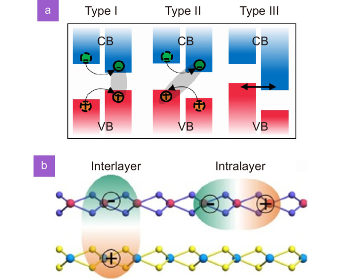
Fig. 1. (a ) Schematic diagram showing the band alignment in type I, II, and III heterostructures. Charge carriers are indicated by circles: green - electrons, orange - holes. Arrows - directions of charge transfer. (b ) Schematic of intra- and interlayer excitons. For interlayer excitons, the electron and the hole are spatially separated into two layers.
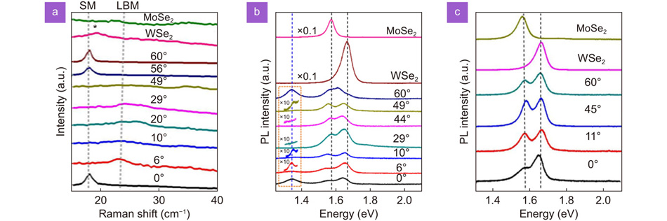
Fig. 2. TMD/TMD heterostructure . (a ) Low frequency Raman spectra of MoSe2/WSe2 HSs and individual TMD layers with different twist angles (0° ≤ θ ≤ 60°) showing the shear mode (SM), layer-breathing mode (LBM), and unassigned peak (marked with asterisk). The pronounced SM at specific twisting angles indicating the strong coupling of the HS at those angles. (b ) PL spectra of the same HS showing the emergence of the interlayer exciton peak at ~ 1.35 eV as a function of different twisting angles. (c ) PL spectra of 1L MoSe2, 1L WSe2, and 1L h-BN-inserted HSs with various twist angles (0° ≤ θ ≤ 60°) showing the absence of the interlayer exciton peak at all twisting angles indicating the reduced coupling between MoSe2 and WSe2. The intensity of the main peaks at the HS are comparable to individual layers further indicating the PL spectra is a combination of each individual material in case of no coupling. Figure reproduced with permission from ref.86, Copyright © 2017, American Chemical Society.
Fig. 3. Perovskite/perovskite heterostructure . (a ) Schematic crystal structures of (PEA)2(MA)n-1PbnX3n+1 perovskites with different n values. n = ∞ - 3D perovskite. (b ) PL spectra of various HSs excited by a 442 nm laser. 527 nm peak corresponds to (PEA)2PbI4 (n = 1), and the 575 nm peak - (PEA)2(MA)Pb2I7 (n = 2). (c ) Optical images of different HSs (from Fig.3 (b) ) under 442 nm. Scale bars are 5 μm. Figure reproduced with permission from ref.150, Copyright © 2018, American Chemical Society.
Fig. 4. Perovskite/TMD heterostructures . (a ) Demonstration of PL enhancement: PL spectra of the 2-layers WS2 (red), and BA2MA3Pb4I13/WS2 heterostructure before (black) and after (blue) interface curing using laser annealing. (b ) Demonstration of PL quenching: PL spectra of the monolayer WS2 (blue), MAPbI3 (green), MAPbI3/WS2 heterostructure (red), the insertion highlights the WS2 peak shift due to trion emission. The asterisk (*) indicates the peak from the sapphire substrate. (c ) PL spectra of the (C6H5C2H4NH3)2PbI4 (PEPI) perovskite (green), 1L WS2 (blue), broadband emission in the perovskite/WS2 heterostructure (red) originated from the interface interlayer excitons at 110 K. Figure reproduced with permission from: (a) ref.93, Copyright © 2019, American Chemical Society; (b) ref.161, Copyright © 2019, American Chemical Society; (c) ref.95, Copyright © 2020, American Chemical Society.
Fig. 5. Schematic illustration of Au-assisted exfoliation PL for the large area TMDs monolayers. (a ) Steps of large area exfoliation of TMDs using Au (TRT stands for thermal release tape). (b ) Schematic of the layer-by-layer exfoliation technique to yield even and odd layers from an AB-stacked vdWs crystal. (c ) Photograph for large area monolayers. (d ) Comparison of PL spectra of Au-assisted exfoliation and traditional exfoliation measured at 4K for different TMDs (top) and intensity distributions (bottom). Black and red colures for Au and Scotch tape–exfoliation, respectively. Figure reproduced with permission from ref.180, Copyright © 2020, AAAS.
Fig. 6. Flow chart for TMDs production via CVD method and comparison with various fabrication strategies for TMDs heterostructures. (a ) General growth process to produce TMDs via CVD. (b ) Comprehensive comparison of various fabrication strategies of TMDs heterostructures. Figure reproduced with permission from: (a) ref.184. Springer Nature; (b) ref.182. John Wiley and Sons.
Fig. 7. (a ) Schematic representation of halide perovskite materials with different dimensionalities ranging from 3D to 0D. (b ) Schematic representation of materials with different degrees of confinement. (c ) Image of colloidal perovskite nanocrystals taken under UV lamp (λ = 365 nm), which feature tunable emission behavior as a function of composition and particle size. (d ) Diagram correlating different thicknesses of PbI2 platelets and the corresponding CH3NH3PbI3 (images below data line) grown on muscovite mica using van der Waals epitaxial growth. Figure reproduced with permission from: (a, b) ref.337, John Wiley and Sons; (c) ref.190, Copyright © 2015, American Chemical Society; (d) ref.188, John Wiley and Sons.
Fig. 8. Perovskites synthesized by different methods. (a ) Photographs of (CH3(CH2)3NH3)2(CH3NH3)n-1PbnI3n+1 crystallites obtained from acid precipitation method. (b ) Schematic illustration of antisolvent vapor-assisted crystallization method. (c ) Optical image of (C6H5CH2CH2NH3)2PbBr4 single crystal obtained from the technique. (d ) Images of a piece of (C6H5CH2CH2NH3)2PbI4 single crystal grown from induced peripheral crystallization (3.5 μm in thickness) that wrapped around a small tube (1.6 cm in diameter; left), demonstrating its flexibility and was used for a flexing angle study (right). (e ) Optical micrograph of exfoliated (C4H9NH3)2PbI4 flakes grown on SiO2/Si substrates. (f ) Optical image of atomically thin 2D (C4H9NH3)2PbBr4 obtained from colloidal method with a scale bar of 10 μm. (g ) Epitaxial (C4H9NH3)2PbI4 flakes deposited on mica by co-evaporation where the two in-plane orientations were marked by red and orange arrows with an offset θ about 9° (center; scale bar of 5 μm)218. Figure reproduced with permission from: (a) ref.203, Copyright © 2016, American Chemical Society; (b, c) ref.204, Copyright © 2017, American Chemical Society; (d) ref.210, under the terms of the Creative Commons CC BY license; (e) ref.211, American Physical Society; (f) ref.147, AAAS; (g) ref.218, John Wiley and Sons © 2017 WILEY‐VCH Verlag GmbH & Co. KGaA, Weinheim.
Fig. 9. Fabrication of TMD-perovskite heterostructures and devices. (a ) Structure models of halide perovskite/MoS2 heterostructure. (b ) False-colored scanning electron microscopy image of evaporated perovskite on MoS2 exhibiting triangular and hexagonal shape. (c ) Optical microscope image of the as fabricated (PEA)2SnI4/MoS2 PD (the scale bar is 20 μm). (d ) Schematics of typical exfoliation and dry transfer process for perovskite/TMD heterostructure fabrication. (e ) Schematic diagram of the facile fabrication process of 2D perovskite/TMD heterostructure with spincoating. Figure reproduced with permission from: (a, b) ref.192, John Wiley and Sons; (c) ref.242. Copyright © 2019, American Chemical Society; (d) ref.93. Copyright © 2019, American Chemical Society; (e) ref.158. John Wiley and Sons.
Fig. 10. (a ) MAPbI3/MoS2/APTES and cross-sectional structure illustration of APTES doping process. (b ) Comparison of the photoresponsivity values of MoS2, MoS2/APTES, and perovskite/MoS2/APTES PDs as a function of wavelength. (c ) Structure of MAPbI3/WS2 PD on sapphire substrate and the relative type-II band alignment. (d ) Spectral responsivity and detectivity of the PD showing its high detectivity. (e ) MAPbI3/MoS2 PD with their relative band alignment (left panel) and charge transfer mechanisms (right panel) using 1T and 2H phases of MoS2. (f ) Responsivity and detectivity values of MAPbI3/1T-MoS2 PD as a function of illumination powers using 500 nm laser. (g –h ) Planar (g), and vertical (h) structures of MAPbI3/MoS2 PDs and the effect of the drain bias and illumination on carrier transportation and separation. (i ) I-V curves of the vertical structure under different power densities showing the photovoltaic characteristics of this hybrid structure. Inset is schematic carrier transportation and separation in this self-power mode. Figure reproduced with permission from: (a, b) ref.239, (c, d) ref.163, (e, f) ref.90, (g–i) ref.256, John Wiley and Sons.
Fig. 11. (a ) MAPbI3/BP/MoS2 and charge transfer mechanism showing both type-I and type-II band alignment at perovskite/BP and BP/MoS2 interfaces, respectively. (b ) The temporal response of MAPbI3/BP/MoS2 hybrid PD, inset shows the measured rise and fall times under 457 nm excitation. (c ) The temporal response of the PD at zero bias mode under different illumination wavelengths. (d , e ) Schematic and relative band diagram of MAPbI3-MoS2 BHJ/rGO PD on SiO2/Si and flexible PEN substrates. (f ) Comparison of the photoresponsivity and detectivity values at 660 nm as a function of illumination intensity of the PD with and without using MoS2 on SiO2/Si substrate. Figure reproduced with permission from: (a–c) ref.91. Copyright © 2019, American Chemical Society; (d–f) ref.257, John Wiley and Sons.
Fig. 12. (a ) Schematic and energy band alignment of CsPbI3-xBrx QDs/MoS2 PD. (b ) Photoresponsivity, specific detectivity, and EQE (inset) of CsPbI3-xBrx QDs/MoS2 PD as a function of illumination powers at 532 nm. (c –e ) Schematic (c), spectral responsivity and corresponding detectivity (d), and temporal photoresponse at 808 nm excitation (e) of Cs-doped FAPbI3/PtSe2 PD. (f –h ) Schematic (f), responsivity and detectivity as a function of illumination intensity at 808 nm (g ), and rise/fall times at 808 nm (h) of Cs-doped FAPbI3/PdSe2 hybrid PD. Figures reproduced/adapted with permission from: (a, b) ref.255, under the terms of the Creative Commons Attribution License; (c–e) ref.278, Copyright © 2018, American Chemical Society; (f–h) ref.279, under the terms of the Creative Commons Attribution License.
Fig. 13. Summary of performance metrics of perovskite/TMD PDs in comparison with commercial PDs. (a ) Current responsivity against response time of perovskite/TMD PDs in comparison with that for the commercial Si and InGaAs. The marked area on the left showing the goal for future development by improving the gain-bandwidth product. (b ) Detectivity comparison between perovskite/TMD PDs and commercial Si and InGaAs PDs. The marked area on the right showing the ultimate target for future development through extending the sensitivity range of the PDs to longer wavelength regime which lacks of candidates with suitable bandgap values. The data for perovskite/TMD PDs were taken from the references shown in Table 4 .
Fig. 14. (a ) Representative J-V curve of PSCs with PEDOT: PSS, MoS2, and WS2 as the hole transporting material. (b ) Plots of PCEs of PSCs based on PEDOT: PSS, MoS2, and WS2 as the function of the storage time. For each group of measurements, 20 cells were adopted for analysis. (c ) The statistic plot for power conversion efficiency of PSCs using different thicknesses of WS2 as the electron transporting material. (d ) EQE spectra and integrated current density (J) of the corresponding devices. Figure reproduced with permission from: (a, b) ref.291, Copyright © 2017, American Chemical Society; (c, d) ref.292, John Wiley and Sons.
Fig. 15. (a ) Schematic diagram of the vdW epitaxial growth of the perovskite crystallizes on a TMD (e.g., WSe2) surface. (b ) Energy-band diagram under flat-band conditions of the fabricated planar inverted PSCs with different materials as the HTL. (c ) J–V curves the best performing PSCs with and without WS2 interlayer. (d ) HRTEM image of one of the MoS2 flakes (synthesized via a solvent-exchange process upon liquid phase exfoliation) oriented in the [001] zone axis having a 2H structure (a sketch of the arrangement of Mo and S atoms in this structure and orientation is superimposed on the HRTEM image). (e ) The cross-sectional TEM image of a PSC with 2D MoS2 nanoflakes acting as HTL buffer layer. The scale bar is 1 μm (f ) Operational stability of PSCs with and without a MoS2 buffer layer302. Figures reproduced/adapted with permission from: (a) ref.295, under the terms of the Creative Commons Attribution License; (b) ref.289, (c) ref.296, (d) ref.301. John Wiley and Sons; (e, f) ref.302, under a Creative Commons Attribution 4.0 International License.
|
Table 0. Key parameters of merits for photodetectors (PDs).
|
Table 0. Synthesis methods of 2D perovskites/TMDs heterostructures.
|
Table 0. Some examples of improved properties by exploiting the heterostructures of perovskite/TMDs.
| ||||||||||||||||||||||||||||||||||||||||||||||||||||||||||||||||||||||||||||||||||||||||||||||||||||||||||||||||||||||||||||||||||||||||||||||||||||||||||||||||||||||||||||||||||||||||||||||||
Table 0. Device performance for several perovskite/TMD hybrid photodetectors (PDs).
| ||||||||||||||||||||||||||||||||||||||||||||||||||||||||||||||||||||||||||||||||||||||||||
Table 0. Device performance for perovskite/TMD solar cells.

Set citation alerts for the article
Please enter your email address
© Copyright 2018-2021 | Chinese Laser Press. All Rights Reserved 沪ICP备15018463号-20