
Yechuan Zhu, Xiaolin Chen, Weizheng Yuan, Zhiqin Chu, Kwok-yin Wong, Dangyuan Lei, Yiting Yu. A waveguide metasurface based quasi-far-field transverse-electric superlens[J]. Opto-Electronic Advances, 2021, 4(10): 210013-1
- Opto-Electronic Advances
- Vol. 4, Issue 10, 210013-1 (2021)
Abstract
Concentrating light into a tiny spot has gained increasingly interests in the field of high-resolution optical imaging. However, the imaging capability of a conventional refractive lens is generally restricted to 0.61λ/NA (λ being the wavelength of light, NA being the numerical aperture of the lens) due to the diffraction of light waves
Recently, we have theoretically designed a superlens formed by an array of metallic nanoslits and demonstrated quasi-far-field super-resolution focusing
![]()
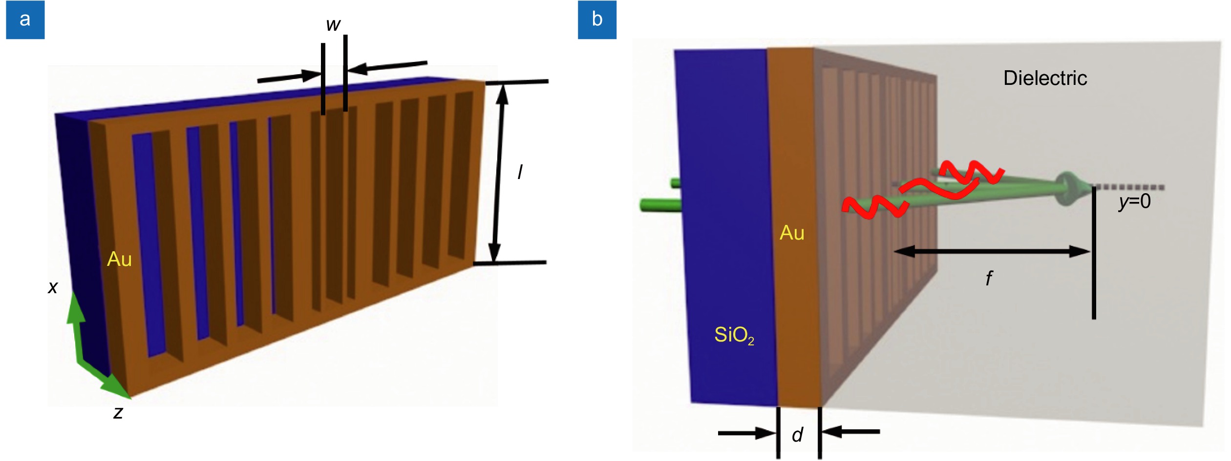
Figure 1.(
![]()
Figure 2.
When a TE-polarized light beam (with polarization parallel to the nanoslits along the x direction) is normally incident upon the superlens from the glass substrate, it can couple with the waveguide modes of the nanoslits, propagate and radiate into the working dielectric domain. Note that each nanoslit can be assumed to be infinite in the x direction when it is longer than 15 µm
where w is the nanoslit width. εm and εd are the relative permittivities of the metal and the dielectric material in the nanoslit, respectively. k is the free-space wavevector. For each TE mode, the propagation constant β can be obtained from Eq. (1). Considering the backward and forward reflections between the input and output interfaces, the electromagnetic field distribution in the ith nanoslit can be expressed in terms of expansion coefficients
where
where
where
Now let us design the superlens to achieve subwavelength focusing. According to the theory of wavefront reconstruction and the principle of equal optical path, the focus at a desired distance f from the superlens can be realized, provided that the phase delay of each nanoslit matches the required phase difference (Δφ(y) – Δφ(0)) as a function of the distance y from the center of the lens, given by
where Δφ(y) is the phase delay of the nanoslit located at the position y, λ is the incident wavelength, p is an arbitrary integer, and nd is the refractive index of the working dielectric for the superlens. Therefore, the phase delay of each nanoslit is the key to the superlens design.
As pointed out in the previous sections, the phase delay of a nanoslit can be predicted by Re(β0)d, where β0 is the propagation constant for the TE0 mode and can be calculated by the following equation deduced from Eq. (1) by setting m = 0:
It can be seen from Eq. (6) that for a specific film thickness d and operating wavelength, the phase delay of a nanoslit can be modulated by the nanoslit width and the working dielectric. On the other hand, by setting the propagation constant to zero, we can find out the cut-off slit width for a TE mode at a given wavelength, below which the mode cannot propagate but decays exponentially with the distance. In one word, the width of a nanoslit should be above the cut-off width for TE0 mode but below that for the TE1 mode to ensure the existence of only TE0 mode in each nanoslit. As a result, the nanoslit width w should meet the following condition:
Based on Eqs. (5) and (7), a superlens immersed in cedar oil with a desired focal length of f = 1.5 µm can be designed with a 200 nm thick gold film at the wavelength of 405 nm. At this wavelength, the permittivity values of gold and cedar oil are −1.6745+5.7286i
To understand the focusing property of the designed superlens, full-wave electromagnetic field simulations were performed using the finite-difference time-domain (FDTD) method. Perfectly matched layers as absorbing boundary conditions were employed around the computational domain. A TE-polarized plane wave was defined by setting the amplitude of the electric field component Ex to be unit. The size for all the grids was uniformly set to be 2 nm both in the transverse y direction and in the longitudinal z direction. The simulated electric field intensity distribution of the superlens is illustrated in Fig. 2(a), which verifies the focusing behavior of the designed superlens by producing a bright subwavelength spot. The simulated focal length of the superlens is 1.484 μm, which is close to the designed value (1.5 μm). Furthermore, according to the intensity distribution at the focal plane of the superlens as illustrated in Fig. 2(b), the full-width at half-maximum (FWHM) of the focus is 98 nm, namely, λ/4.13, well beyond the diffraction limit of 170 nm (calculated by 0.61λ/NA, namely, λ/2.38). Therefore, a super-resolution focus with a focal length of 3.66λ is realized by the superlens. Moreover, the simulated transmission efficiency of the superlens is about 40.2% and the maximum intensity in the focal plane of the focus is 4.03 times larger than the incident intensity. In addition, we also calculated the electric field distribution profiles both in the working dielectric domain (Fig. 2(d)) and at the focal plane (Fig. 2(e)) using the analytical solutions given by Eq. (3). It can be seen that the results agree well with the FDTD simulation results. For simplicity, here the modal amplitude on the exit surface of each nanoslit is obtained by interpolating with the FDTD simulated electric field.
To explore the underlying mechanism of the proposed superlens working in the quasi-far field, we did a special Fourier transformation for the FDTD simulated electromagnetic waves along the y direction. The corresponding Fourier spectrum of electric field as a function of spatial frequency ky (the wavevector in y direction) and position z are given in Fig. 2(c). The blue and green dashed lines mark the positions of the normalized cut-off frequency of conventional lenses NA/nd (≈ 0.96) and working dielectric k0 (k0 = 2πnd/λ), respectively. From Fig. 2(c), we can see that some considerable high-spatial-frequency components with ky > k0, i.e. beyond the cut-off spatial frequency of working dielectric, locate at the focal spot. And more components with ky > k0NA/nd are generated at the exit plane of the superlens (at z=0 μm). These results indicate there are some high-spatial-frequency waves generated and amplified by the superlens. Therefore, the superlens not only provides the components with ky < k0NA/nd, but also brings the high-spatial-frequency components with ky > k0NA/nd, which are normally lost in the foci of traditional refractive lenses, thus leading to the super-resolution focusing of the superlens beyond the diffraction limit. Moreover, the theoretically calculated angular spectrum of electric field is given in Fig. 2(f), which agrees very well with the numerical results.
After having explored the underlying physics, we performed the experimental work to demonstrate the proposed superlens. Specifically, the superlens was fabricated with the following processes. First, the glass substrate was cleaned using acetone in an ultrasonic bath for 10 minutes. After cleaning, the substrate was washed with the de-ionized water and then dried. Then, a 200 nm thick gold film as a function layer was deposited on the glass substrate using electron beam evaporation (pressure <4×10 −4 Pa; deposition rate: 2 Å/s (1Å=10−10 m)). Finally, the gold film was nanopatterned by milling through the film using focused ion beam (FIB) (acceleration voltage: 30 kV; Ga+ ion beam current: 80 pA). The resulting structure of the superlens was imaged by scanning electron microscope (SEM), as shown in Fig. 3(a).
![]()
Figure 3.
We characterized the focusing performance of the fabricated superlens using a Nikon inverted microscope (Nikon Eclipse Ti-U) with oil immersed objective (Nikon CFI LU Plan APO EPI 100×, NA=0.9). In our optical experiment, a 405 nm laser was used as the illumination source and expanded to achieve a uniformly distributed beam. After expansion, the uniform beam was polarized parallel to the nanoslits with a linear polarizer (Thorlabs, LPVISE100-A) to achieve a TE-polarized incidence and then irradiated upon the superlens, and the incident beam could be considered locally as a plane wave since the illumination spot was much larger than the size of the superlens structure. A Nikon inverted microscope was employed to find the exit plane of the superlens and collect the transmitted light. Then, the light emitted from the superlens was recorded using a high-resolution CCD camera (Olympus, 2560×1280, the mesh size in the image processing software is 30 nm) driven by a piezo-electrical stage with an axial moving resolution of 10 nm (Physik Instrument, E-816). After fine tuning 400 steps, the intensity distribution of the “focused” superlens was measured, as shown in Fig. 3(b). It is worth noting that we should ensure the light source to be perpendicular to the device in the experiment, since the error in perpendicularity has a great influence on the focusing behavior of the superlens.
As can be seen from Fig. 3(b), the experimentally measured focal length of the superlens is 1.49 μm (3.68λ), which is very close to the designed value of 1.5 μm. Furthermore, according to the intensity distribution at the focal plane of the superlens as illustrated in Fig. 3(c), the experimentally measured FWHM of the superlens also agrees very well with the simulated result. The FWHMs are all 98 nm, namely λ/4.13, which is beyond the diffraction limit of λ/2.38. Therefore, quasi-far-field super-resolution focusing based on the TE superlens is experimentally verified. It is noted that the superlens we developed demonstrates great advantages over the transverse-magnetic (TM) lens which can also operate in the far-field zone
In conclusion, we have designed a quasi-far-field super-resolution focusing superlens consisting of nanoslits milled in a gold film via the excitation of TE waveguide modes working at a visible wavelength region. Mean-while, the experimental measurements on the fabricated superlens show excellent agreements with the numerical simulations, being consistent with our theoretical predictions. More importantly, our superlens can not only provide low-spatial-frequency components, but also bring high-spatial-frequency components that are normally lost in the foci of traditional refractive lenses. The latter is the key to overcome the diffraction limit for the super-resolution focusing using our superlens. Further-more, the proposed method can be promoted to construct focusing devices beyond the diffraction limit at other wavelengths. Our first experimental demonstration is a crucial step in the realization of this super-resolution focusing technology for many potential applications in optoelectronics and biomedical imaging.
References
[1] On the theory of optical images, with special reference to the microscope. London, Edinb, Dublin Philos Mag J Sci, 42, 167-195(1896).
[2] Superlenses to overcome the diffraction limit. Nat Mater, 7, 435-441(2008).
[3] Negative refraction makes a perfect lens. Phys Rev Lett, 85, 3966-3969(2000).
[4] Sub-diffraction-limited optical imaging with a silver superlens. Science, 308, 534-537(2005).
[5] Maskless plasmonic lithography at 22 nm resolution. Sci Rep, 1, 175(2011).
[6] Nanofocusing of electromagnetic radiation. Nat Photon, 8, 13-22(2014).
[7] Plasmonic lenses formed by two-dimensional nanometric cross-shaped aperture arrays for Fresnel-region focusing. Nano Lett, 10, 1936-1940(2010).
[8] Beam manipulating by metallic nano-slits with variant widths. Opt Express, 13, 6815-6820(2005).
[9] Planar lenses based on nanoscale slit arrays in a metallic film. Nano Lett, 9, 235-238(2009).
[10] Effect of lens size on the focusing performance of plasmonic lenses and suggestions for the design. Opt Express, 19, 9434-9444(2011).
[11] Theory and implementation of focal shift of plasmonic lenses. Opt Lett, 37, 1592-1594(2012).
[12] Metallic planar lens formed by coupled width-variable nanoslits for superfocusing. Opt Express, 23, 20124-20131(2015).
[13] Light propagation with phase discontinuities: generalized laws of reflection and refraction. Science, 334, 333-337(2011).
[14] Broadband light bending with plasmonic nanoantennas. Science, 335, 427(2012).
[15] Dielectric gradient metasurface optical elements. Science, 345, 298-302(2014).
[16] Multiwavelength achromatic metasurfaces by dispersive phase compensation. Science, 347, 1342-1345(2015).
[17] Metalenses at visible wavelengths: diffraction-limited focusing and subwavelength resolution imaging. Science, 352, 1190-1194(2016).
[18] Meta-lens doublet in the visible region. Nano Lett, 17, 4902-4907(2017).
[19] A broadband achromatic metalens for focusing and imaging in the visible. Nat Nanotechnol, 13, 220-226(2018).
[20] A broadband achromatic metalens in the visible. Nat Nanotechnol, 13, 227-232(2018).
[21] All-glass, large metalens at visible wavelength using deep-ultraviolet projection lithography. Nano Lett, 19, 8673-8682(2019).
[22] TE-polarized design for metallic slit lenses: a way to deep-subwavelength focusing over a broad wavelength range. Opt Lett, 43, 206-209(2018).
[23] Investigation on super-resolution focusing performance of a TE-polarized nanoslit-based two-dimensional lens. Nanomaterials, 10, 3(2020).
[24] Optical transmission through subwavelength slit apertures in metallic films. Opt Commun, 280, 10-15(2007).
[25] Light passing through subwavelength apertures. Rev Mod Phys, 82, 729-787(2010).
[26] Optical resonance in a narrow slit in a thick metallic screen. Phys Rev Lett, 86, 5601-5603(2001).
[27] Optical constants of the noble metals. Phys Rev B, 6, 4370-4379(1972).

Set citation alerts for the article
Please enter your email address
© Copyright 2018-2021 | Chinese Laser Press. All Rights Reserved 沪ICP备15018463号-20