
Jianping ZHANG, Jing ZHANG, Zhiqiang WANG, Wuli⁃Jibaier TANG, Yezhou FANG, Jianyun XIE, Hailin XUE, Liang YAN. Study on Separation Mechanism of Gamma Curve in Screen[J]. Optoelectronic Technology, 2023, 43(2): 186
- Optoelectronic Technology
- Vol. 43, Issue 2, 186 (2023)

Fig. 1. Gamma curve separation phenomenon
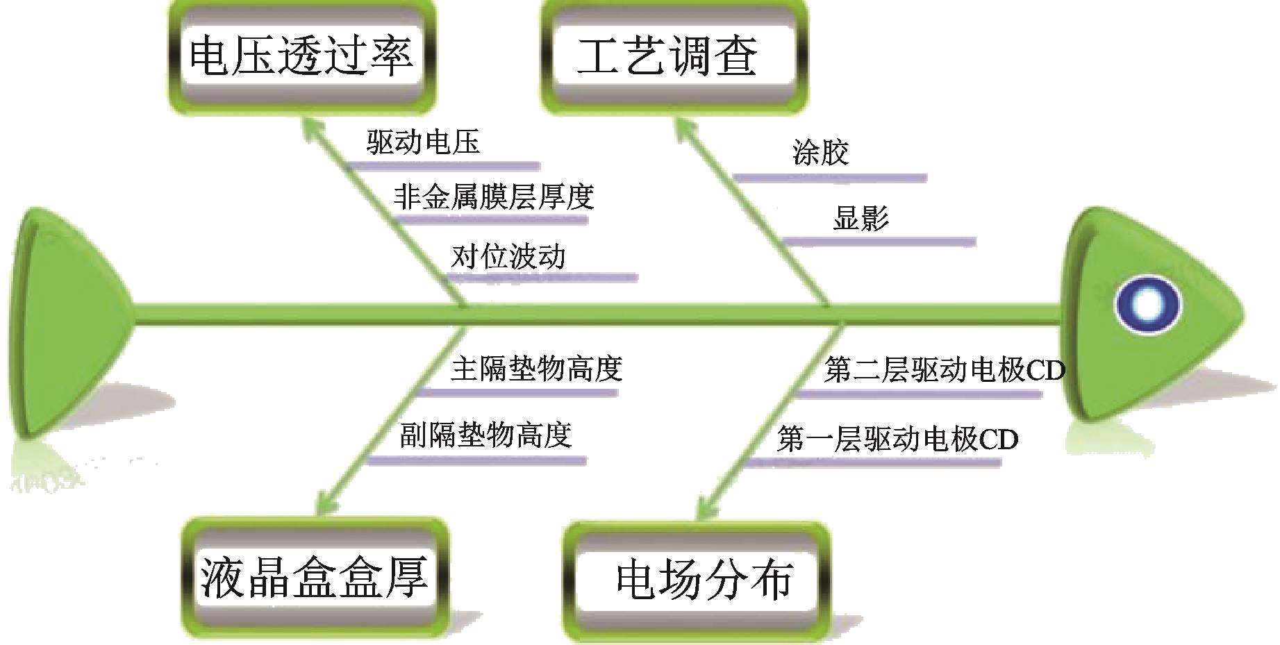
Fig. 2. Gamma curve separation impact factors
Fig. 3. The actual alignment level of the upper and lower screens
Fig. 4. Cell Gap difference between upper and lower screens
Fig. 5. Thickness of upper and lower screen capacitor dielectric layer
Fig. 6. A single product difference of the pixel electrode CD between the upper and lower screen of the whole glass
Fig. 7. CD difference between normal condition and reverse exposure electrode
Fig. 8. CD difference between normal condition and reverse gluing electrode
Fig. 9. CD difference between normal condition and reverse developing electrode
Fig. 10. Glue starting position
Fig. 11. The lower height of PS at the starting position of gluing
Fig. 12. Upper screen pixel electrode with larger pixel structure
Fig. 13. Lower screen pixel electrode with smaller pixel structure
Fig. 14. Relationship curve of voltage and transmittance
Fig. 15. Improved uniformity of drive field
Fig. 16. Gamma curve improvement
|
Table 1. Thickness contrast between the upper and lower screen boxes before and after closing

Set citation alerts for the article
Please enter your email address
© Copyright 2018-2021 | Chinese Laser Press. All Rights Reserved 沪ICP备15018463号-20