• Laser & Optoelectronics Progress
  • Vol. 61, Issue 10, 1012004 (2024)
Shunqin Xu, Lihong Yang*, Qinyue Fu, Qianxi Chen, Xingyuan Li, and Hang Ge
Author Affiliations
  • College of Photoelectric Engineering, Xi'an Technological University, Xi'an, 710021, Shaanxi, China
  • show less
    DOI: 10.3788/LOP232084 Cite this Article Set citation alerts
    Shunqin Xu, Lihong Yang, Qinyue Fu, Qianxi Chen, Xingyuan Li, Hang Ge. Visual Detection Method of Optical Lens Surface Defect Under Dual Light Sources[J]. Laser & Optoelectronics Progress, 2024, 61(10): 1012004 Copy Citation Text show less
    Structure of the critical defect detection device
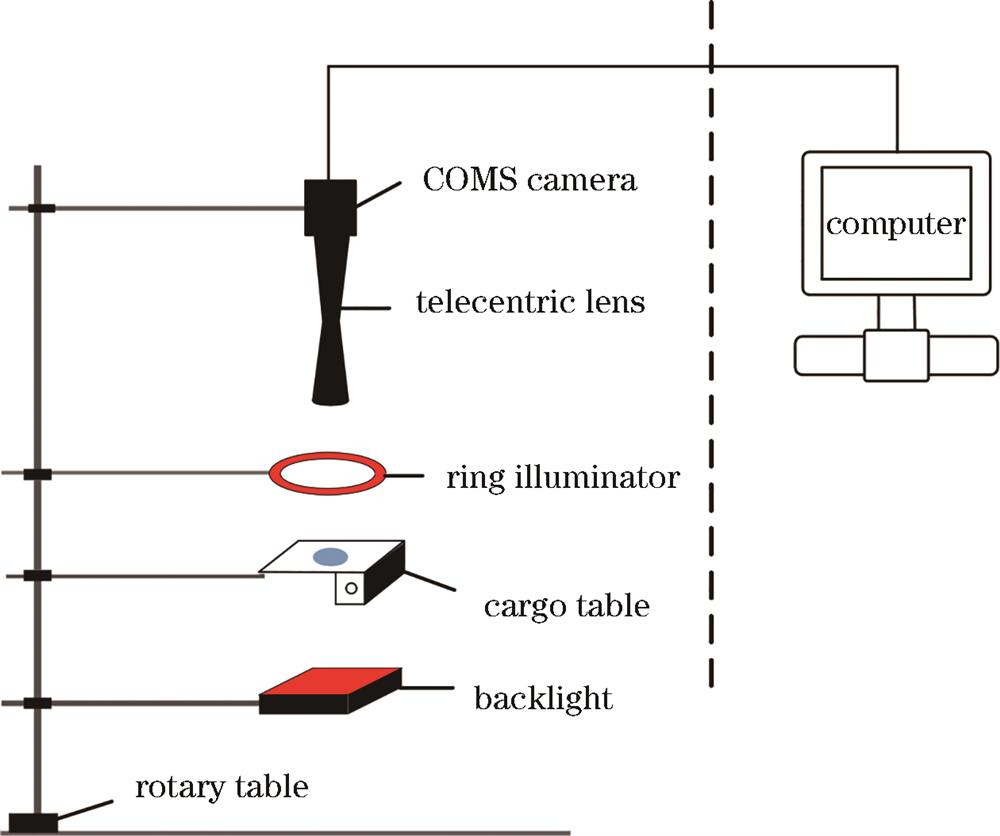
    Fig. 1. Structure of the critical defect detection device
    Images acquired from the lenses under different illumination. (a) Surface image collected under forward light; (b) surface image collected under backlight
    Fig. 2. Images acquired from the lenses under different illumination. (a) Surface image collected under forward light; (b) surface image collected under backlight
    Telecentric lens imaging features
    Fig. 3. Telecentric lens imaging features
    Two light source illumination modes. (a) Ring-light source illumination mode; (b) parallel backlight source illumination mode
    Fig. 4. Two light source illumination modes. (a) Ring-light source illumination mode; (b) parallel backlight source illumination mode
    Flow chart of image processing
    Fig. 5. Flow chart of image processing
    Images acquired from optical lenses under different light sources. (a) Forward light defect image; (b) backlight defect image
    Fig. 6. Images acquired from optical lenses under different light sources. (a) Forward light defect image; (b) backlight defect image
    Preprocessed defect images. (a) Defects identified in forward light; (b) defects identified in backlight; (c) defects identified after image fusion
    Fig. 7. Preprocessed defect images. (a) Defects identified in forward light; (b) defects identified in backlight; (c) defects identified after image fusion
    Calibration parameters of the imaging system
    A single pixel wide(Sx)/μm3.44961Center point y coordinates(Cy)/pixel1024.02
    A single pixel high(Sy)/μm3.45Medium image wide /pixel2448
    Magnification /times0.801082Medium image high /pixel2048
    X rotation direction /(°)357.985Y rotation direction /(°)358.914
    Center point x coordinates(Cx)/pixel1223.81Z rotation direction /(°)3.24858
    Table 1. Calibration parameters
    NumberDefectZYGO interferometer /μmSystem test /μmError ratio /%
    WidthDiameterWidthDiameter
    1Pitting17.48417.6951.206
    2Pitting7.5967.3942.659
    3Pitting42.32541.9750.826
    4Pitting53.23553.2970.116
    5Pitting96.53396.5050.029
    6Scratch8.4128.4300.214
    7Scratch15.19615.3030.704
    8Scratch28.49528.5510.196
    9Scratch37.62337.6270.011
    10Scratch67.76967.8920.181
    Table 2. Error analysis
    Detection methodTotal number of defectNumber of pitingNumber of scratch
    Forward light detection15510
    Backlight detection1486
    Image fusion detection251312
    Table 3. Lens defect detection results
    Detection methodScratch maximum width /μmScratch minimum width /μmPiting maximum diameter /μmPiting minimum diameter /μmTime /s
    System713.80823.80063.29734.0355.327
    ZYGO713.62524.57563.39834.021304.000
    Manual710.00030.00060.00030.000
    Table 4. Comparison among system detection results, ZYGO detection results and manual detection results
    Shunqin Xu, Lihong Yang, Qinyue Fu, Qianxi Chen, Xingyuan Li, Hang Ge. Visual Detection Method of Optical Lens Surface Defect Under Dual Light Sources[J]. Laser & Optoelectronics Progress, 2024, 61(10): 1012004
    Download Citation