• Chinese Journal of Lasers
  • Vol. 48, Issue 11, 1100001 (2021)
Jiang Wang and Linbao Luo*
Author Affiliations
  • School of Electronic Science and Applied Physics, Hefei University of Technology, Hefei, Anhui 230009, China
  • show less
    DOI: 10.3788/CJL202148.1100001 Cite this Article Set citation alerts
    Jiang Wang, Linbao Luo. Advances in Ga2O3-Based Solar-Blind Ultraviolet Photodetectors[J]. Chinese Journal of Lasers, 2021, 48(11): 1100001 Copy Citation Text show less
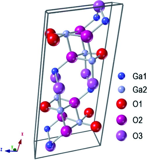
    Crystal structure of β-Ga2O3[45]
    Fig. 1. Crystal structure of β-Ga2O3[45]
    Morphology of β-Ga2O3 nanowires and photoelectric response of device[152]. (a) SEM image of the β-Ga2O3 nanowires grown on the Au-coated silicon substrate; (b) I-V curves of the detector under 254 nm light illumination and dark condition (inset); (c) time response of the device to light at 254 nm; (d) enlargement of the rising and falling edges for the light “on” and “off” for the first time
    Fig. 2. Morphology of β-Ga2O3 nanowires and photoelectric response of device[152]. (a) SEM image of the β-Ga2O3 nanowires grown on the Au-coated silicon substrate; (b) I-V curves of the detector under 254 nm light illumination and dark condition (inset); (c) time response of the device to light at 254 nm; (d) enlargement of the rising and falling edges for the light “on” and “off” for the first time
    Structural characteristics of Ga2O3 and performance of the device[135]. (a) X-ray diffraction (XRD) pattern of the α-Ga2O3 grown on the sapphire substrate. The inset shows the schematic of the device structure; (b) spectral responsivity of the photodetectors at 5 V bias; (c) I-V characteristics of the devices in the dark (black line) and under illumination
    Fig. 3. Structural characteristics of Ga2O3 and performance of the device[135]. (a) X-ray diffraction (XRD) pattern of the α-Ga2O3 grown on the sapphire substrate. The inset shows the schematic of the device structure; (b) spectral responsivity of the photodetectors at 5 V bias; (c) I-V characteristics of the devices in the dark (black line) and under illumination
    Structure and electrical characteristics of the device based on β-Ga2O3 flake[72]. (a) Schematic of the preparation process of the β-Ga2O3 flake based solar-blind photodetector; (b) optical microscopy image of the device; (c) typical electrical properties of the β-Ga2O3 flake based FETs; (d) time-dependent photoresponse of the photodetector under illumination at different wavelengths; (e) responsivity as a function of wavelength
    Fig. 4. Structure and electrical characteristics of the device based on β-Ga2O3 flake[72]. (a) Schematic of the preparation process of the β-Ga2O3 flake based solar-blind photodetector; (b) optical microscopy image of the device; (c) typical electrical properties of the β-Ga2O3 flake based FETs; (d) time-dependent photoresponse of the photodetector under illumination at different wavelengths; (e) responsivity as a function of wavelength
    Ga2O3 photodetector and its performance test. (a) Fabrication process of photodetector[142]; (b) current-voltage (I-V) characteristics of photodetector. Filled and hollow dots represent current in the dark condition and 250 nm-light irradiationv, respectively[142]; (c) responsivity and photocurrent response of the photodetector at reverse bias of 10 V[142]; (d) photograph of the flame detector[162]; (e) transient response of the detector[162]; (f) signal from the flame detection system[162]
    Fig. 5. Ga2O3 photodetector and its performance test. (a) Fabrication process of photodetector[142]; (b) current-voltage (I-V) characteristics of photodetector. Filled and hollow dots represent current in the dark condition and 250 nm-light irradiationv, respectively[142]; (c) responsivity and photocurrent response of the photodetector at reverse bias of 10 V[142]; (d) photograph of the flame detector[162]; (e) transient response of the detector[162]; (f) signal from the flame detection system[162]
    Performance of the Ga2O3 Schottky photodiode[18]. (a) Dark I-V characteristics of the Au-Ga2O3 Schottky photodiode annealed at various temperatures; (b) spectral response of the device before and after annealing
    Fig. 6. Performance of the Ga2O3 Schottky photodiode[18]. (a) Dark I-V characteristics of the Au-Ga2O3 Schottky photodiode annealed at various temperatures; (b) spectral response of the device before and after annealing
    Crystal wafer of Ga2O3 and time response of the device[163]. (a)(b) Epitaxial wafer and AFM image of the Ga2O3; (c) time response of the photodetector with the β-Ga2O3 MSM structure
    Fig. 7. Crystal wafer of Ga2O3 and time response of the device[163]. (a)(b) Epitaxial wafer and AFM image of the Ga2O3; (c) time response of the photodetector with the β-Ga2O3 MSM structure
    Configuration and its photoresponse of the narrow-band detector based on β-Ga2O3 single crystal[166]. (a) AFM image of the (100) β-Ga2O3 single crystal; (b) configuration of the narrow-band detector combined with an orthogonally aligned filter; (c) photoresponsivity as a function of chopper modulation frequency; (d) fitting of waveform curves of transient photoresponse measured at 150 Hz
    Fig. 8. Configuration and its photoresponse of the narrow-band detector based on β-Ga2O3 single crystal[166]. (a) AFM image of the (100) β-Ga2O3 single crystal; (b) configuration of the narrow-band detector combined with an orthogonally aligned filter; (c) photoresponsivity as a function of chopper modulation frequency; (d) fitting of waveform curves of transient photoresponse measured at 150 Hz
    Schematic diagram and measured I-V characteristic curves of the fabricated β-Ga2O3 photodetector. (a) Schematic diagram of the fabricated β-Ga2O3 photodetector; (b) measured I-V characteristic curves
    Fig. 9. Schematic diagram and measured I-V characteristic curves of the fabricated β-Ga2O3 photodetector. (a) Schematic diagram of the fabricated β-Ga2O3 photodetector; (b) measured I-V characteristic curves
    Structural schematic of the device and its spectral response [168]. (a) Structural schematic of β-Ga2O3 single-crystal photodiode; (b) spectral response of Ga2O3 photodiodes with and without a cap layer at reverse and forward biases of 3 V
    Fig. 10. Structural schematic of the device and its spectral response [168]. (a) Structural schematic of β-Ga2O3 single-crystal photodiode; (b) spectral response of Ga2O3 photodiodes with and without a cap layer at reverse and forward biases of 3 V
    PL spectra of Ga2O3 films. (a) NIR PL spectra of Er∶Ga2O3 films with different concentrations[171]; (b) PL spectra of Ce∶Ga2O3 films with different doping concentrations[174]
    Fig. 11. PL spectra of Ga2O3 films. (a) NIR PL spectra of Er∶Ga2O3 films with different concentrations[171]; (b) PL spectra of Ce∶Ga2O3 films with different doping concentrations[174]
    Electrical characteristics and spectral response of Ga2O3 solar-blind photodetectors. (a) I-V characteristics of the annealed β-Ga2O3 thin film at 800 ℃[184]; (b) I-V curves of the MSM ε-Ga2O3 photodetector in the dark at variable temperatures[136]; (c) R and D* as functions of the wavelength of the MSM ε-Ga2O3 photodetector at a bias of 6 V[136]; (d) magnified fall edge of the I-t characteristic curves[136]
    Fig. 12. Electrical characteristics and spectral response of Ga2O3 solar-blind photodetectors. (a) I-V characteristics of the annealed β-Ga2O3 thin film at 800 ℃[184]; (b) I-V curves of the MSM ε-Ga2O3 photodetector in the dark at variable temperatures[136]; (c) R and D* as functions of the wavelength of the MSM ε-Ga2O3 photodetector at a bias of 6 V[136]; (d) magnified fall edge of the I-t characteristic curves[136]
    I-V characteristics and spectral response of the device. (a) Current-voltage characteristics for various UV-light illumination intensities[208]; (b) schematic diagram of the APD[150]; (c) I-V characteristics of the device[150]; (d) spectral response of the device at -6 V bias[150]
    Fig. 13. I-V characteristics and spectral response of the device. (a) Current-voltage characteristics for various UV-light illumination intensities[208]; (b) schematic diagram of the APD[150]; (c) I-V characteristics of the device[150]; (d) spectral response of the device at -6 V bias[150]
    Principle of photoresponse and spectral response of the device. (a) Normalized transient photoresponse characteristics at room temperature[212]; (b) photoconductive gain and avalanche multiplication gain for the device as functions of applied bias[212]; (c) energy band diagram at high reverse bias under 254 nm illumination[212]; (d) HRTEM images acquired from sample[214]; (e) pulse photocurrent as a function of the time of the Ga2O3 thin-film photodetectors[214]; (f) spectral responsivity of the device at bias of 5 V[214]
    Fig. 14. Principle of photoresponse and spectral response of the device. (a) Normalized transient photoresponse characteristics at room temperature[212]; (b) photoconductive gain and avalanche multiplication gain for the device as functions of applied bias[212]; (c) energy band diagram at high reverse bias under 254 nm illumination[212]; (d) HRTEM images acquired from sample[214]; (e) pulse photocurrent as a function of the time of the Ga2O3 thin-film photodetectors[214]; (f) spectral responsivity of the device at bias of 5 V[214]
    Fabrication process and photoelectric properties of β-Ga2O3 nanowires photodiode[145]. (a) Schematic illustration of the fabrication of β-Ga2O3 nanowires array film and its vertical Schottky photodiode; (b) I-V characteristics of device in dark and under the illumination at 254 nm; (c) spectral response of the device
    Fig. 15. Fabrication process and photoelectric properties of β-Ga2O3 nanowires photodiode[145]. (a) Schematic illustration of the fabrication of β-Ga2O3 nanowires array film and its vertical Schottky photodiode; (b) I-V characteristics of device in dark and under the illumination at 254 nm; (c) spectral response of the device
    Imaging and photoresponse of β-Ga2O3 photodetectors. (a) Spectral response of the diamond/β-Ga2O3 photodetector at 0 V bias[148]; (b) image of the object with letters “UV” on a black paper and the image obtained from the imaging system[148]; (c) I-V curves of the MoS2/β-Ga2O3 heterojunction device[151]; (d) time-dependent photoresponse of the device[151]; (e) typical PEC system built for evaluating the photoresponse behaviors of the α-Ga2O3 NA/Cu2O photodetector[227]; (f) transient response current for the photodetector at zero bias[227]
    Fig. 16. Imaging and photoresponse of β-Ga2O3 photodetectors. (a) Spectral response of the diamond/β-Ga2O3 photodetector at 0 V bias[148]; (b) image of the object with letters “UV” on a black paper and the image obtained from the imaging system[148]; (c) I-V curves of the MoS2/β-Ga2O3 heterojunction device[151]; (d) time-dependent photoresponse of the device[151]; (e) typical PEC system built for evaluating the photoresponse behaviors of the α-Ga2O3 NA/Cu2O photodetector[227]; (f) transient response current for the photodetector at zero bias[227]
    Spectral response and impulse response of β-Ga2O3 photodetector. (a) Photocurrent and power density as functions of excitation wavelength[230]; (b) spectral response of reference β-Ga2O3 photodetector at 1V bias and β-Ga2O3/PANI at zero bias[230]; (c) spectral responsivity and corresponding absorption spectrum of the photodetector[233]; (d) time response of the photodetector for the 248nm pulse laser without bias[233]
    Fig. 17. Spectral response and impulse response of β-Ga2O3 photodetector. (a) Photocurrent and power density as functions of excitation wavelength[230]; (b) spectral response of reference β-Ga2O3 photodetector at 1V bias and β-Ga2O3/PANI at zero bias[230]; (c) spectral responsivity and corresponding absorption spectrum of the photodetector[233]; (d) time response of the photodetector for the 248nm pulse laser without bias[233]
    PolymorphLattice constant /(10-10 m)Bandgap /eVStructureSpace groupOptical dielectricconstant
    αa,b=4.98--5.04,c=13.4--13.605.3RhombohedralR3¯c3.03--3.80
    βa=12.12--12.34,b=3.03--3.04,c=5.80--5.874.2--4.9MonoclinicC2/m2.82--3.57
    γa=8.24--8.305.0CubicFd3¯m-
    δa=9.40--10.0CubicIa3¯-
    εa=5.06--5.12,b=8.69--8.79,c=9.30--9.404.9HexagonalP63mc-
    Table 1. Summary of basic parameters of Ga2O3 polycrystalline[15,42]
    ParameterSiGaAsGaN4H-SiCMgZnODiamondβ-Ga2O3
    Bandgap Eg/eV1.101.433.403.253.70--7.805.504.20--4.90
    Relative dielectric constant ε11.812.99.09.74.65.5010.0
    Breakdown field /(MV·cm-1)0.30.43.32.5-10.08.0
    Electron mobility /(cm2·V-1·s-1)14808400125010002502000300
    Thermal conductivity /(W·cm-1 ·K)1.50.52.34.91.220.00.1--0.3
    Saturation velocity (107 cm·s-1)11.22.52-11.8--2
    Baliga (ε·μ·Ec3)114.7846317-246603444
    Keyes[λ/(4πε)]1/210.31.83.6-41.50.2
    Table 2. Properties of β-Ga2O3 and other more commonly used semiconductors[55]
    Growth MethodMaterialId/nAR /(A·W-1)EQE /%tr /std /sRef. NoYear
    MBEβ-Ga2O3 film128--0.861.02[94]2014
    β-Ga2O3 film45--0.620.83[183]2014
    β-Ga2O3 film0.04259>1040.40.1[96]2015
    Mn∶β-Ga2O3 film842.10.07360.910.28[191]2016
    β-Ga2O3 film70153-510.3[192]2017
    β-Ga2O3 film101.5-3.30.4[5]2017
    β-Ga2O3 film0.02654.9-24[193]2017
    β-Ga2O3 film7.310-50.5--[194]2018
    β-Ga2O3 film-8.41-2.970.41[195]2019
    Growth MethodMaterialId/nAR /(A·W-1)EQE /%tr /std /sRef. NoYear
    RFMSβ-Ga2O3 film4043.31>1041.080.65[121]2017
    Ga2O3 film0.3470.26-0.410.02[178]2017
    Mg∶β-Ga2O3 film~10-30.024-0.330.02[60]2017
    Ga2O3 film-0.19-<10-5<10-5[139]2017
    β-Ga2O3 film10-30.8934440.310.25[137]2018
    β-Ga2O3 film7.632.60212650.261.00[124]2018
    Ga2O3 film~10-3436.3-~10-8~10-4[196]2019
    Ga2O3 film1630055.5--~10-4[197]2019
    β-Ga2O3 film~10-2144.4664711~10-8~10-5[144]2019
    Ga2O3 film0.178.94450~10-3[138]2019
    PLDβ-Ga2O3 film~10-33.7---[198]2018
    β-Ga2O3 film2.50.33-~10-6<10-4[199]2018
    β-Ga2O3 film2.820.415197.8--[200]2019
    MOCVDβ-Ga2O3 film3426.1>1040.480.18[201]2017
    Zn∶β-Ga2O3 film10>103-4.50.8[62]2017
    β-Ga2O3 film12.812.8-~10-3~10-3[115]2018
    β-Ga2O3 film~10-4150>1041.80.3[182]2018
    Zn∶Ga2O3 film~10-41.055124.52.2[202]2018
    Mg∶Ga2O3 film0.528.943410.160.14[103]2019
    β-Ga2O3 film-46>104~10-6~10-5[184]2019
    ε-Ga2O3 film0.023230>105-0.024[136]2020
    β-Ga2O3 film~10-33930.55928790.1950.091[203]2020
    ALDβ-Ga2O3 film0.245.11-~10-6-[110]2017
    α-Ga2O3 film~10-30.76-~10-7<10-4[204]2018
    α-Ga2O3 film0.1631.2---[205]2019
    Ga2O3 film~0.011.34--~10-7[206]2020
    Table 3. Summary of parameters of Ga2O3 thin films based photodetectors
    Jiang Wang, Linbao Luo. Advances in Ga2O3-Based Solar-Blind Ultraviolet Photodetectors[J]. Chinese Journal of Lasers, 2021, 48(11): 1100001
    Download Citation