• Photonics Research
  • Vol. 9, Issue 9, 1734 (2021)
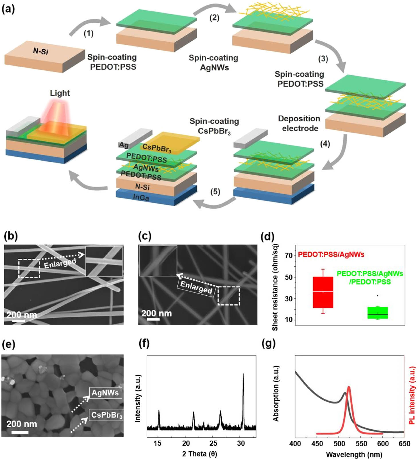
Yujin Liu1, Zhong Ji1、3、*, Yaping Li1, Hong Jin Fan2, and Wenjie Mai1、4、*
Author Affiliations
  • 1Department of Physics, Jinan University, Guangzhou 510632, China
  • 2School of Physical and Mathematical Sciences, Nanyang Technological University, Singapore 637371, Singapore
  • 3e-mail: jizhong@jnu.edu.cn
  • 4e-mail: wenjiemai@email.jnu.edu.cn
  • show less
    DOI: 10.1364/PRJ.411415 Cite this Article Set citation alerts
    Yujin Liu, Zhong Ji, Yaping Li, Hong Jin Fan, Wenjie Mai. Spectrum-shaped Si-perovskite hybrid photodetectors for hyperspectral bioimaging[J]. Photonics Research, 2021, 9(9): 1734 Copy Citation Text show less
    Fabrication steps of Si−CsPbBr3 hybrid PD and materials characterization. (a) Schematic of the fabrication process of the Si−CsPbBr3 hybrid PD. (b), (c) Scanning electron microscopy (SEM) images of the PEDOT:PSS/AgNWs (PA) film and PEDOT:PSS/AgNWs/PEDOT:PSS composite layer (PAP-CL), respectively. (d) Sheet resistance of the PA and PAP-CL. (e) Top-view SEM image of the PAP-CL decorated with a CsPbBr3 perovskite layer. (f) X-ray diffraction (XRD) pattern of the CsPbBr3 perovskite film on FTO. (g) Absorbance and photoluminescence (PL) spectra of the CsPbBr3 perovskite film.
    Fig. 1. Fabrication steps of SiCsPbBr3 hybrid PD and materials characterization. (a) Schematic of the fabrication process of the SiCsPbBr3 hybrid PD. (b), (c) Scanning electron microscopy (SEM) images of the PEDOT:PSS/AgNWs (PA) film and PEDOT:PSS/AgNWs/PEDOT:PSS composite layer (PAP-CL), respectively. (d) Sheet resistance of the PA and PAP-CL. (e) Top-view SEM image of the PAP-CL decorated with a CsPbBr3 perovskite layer. (f) X-ray diffraction (XRD) pattern of the CsPbBr3 perovskite film on FTO. (g) Absorbance and photoluminescence (PL) spectra of the CsPbBr3 perovskite film.
    Mechanism analysis of spectrum shaping. (a)–(d) Testing diagrams of Si−CsPbBr3 hybrid PD (device#1), Si/CsPbBr3 PD (device#2), Si/PAP-CL PD (device#3), and Si/PAP PD with a CsPbBr3 shielding layer (device #4), respectively. (e) Spectral responsivity curves (300–1100 nm) of above four devices. (f) Reflectance spectra of Si and Si/PAP-CL/CsPbBr3 wafers. (g), (h) Ultraviolet photoelectron spectroscopy (UPS) spectra of CsPbBr3 on Si or on PAP-CL with the binding energy secondary-electron cutoffs and HOMO regions. (i) Schematic diagram of the energy band alignment of Si, CsPbBr3, and PEDOT:PSS. (j) The corresponding band bending diagram of device#1, 2, and 3.
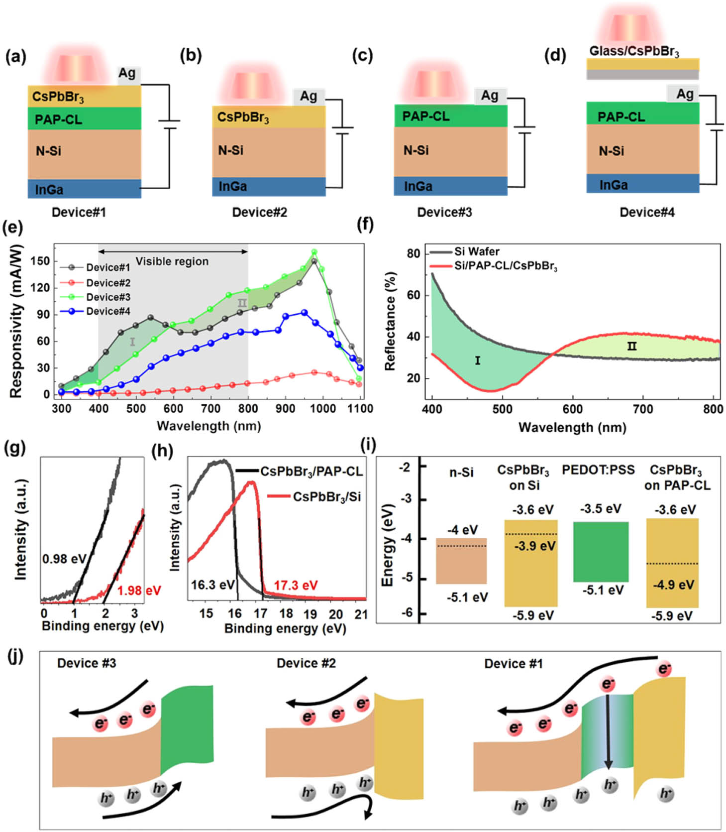
    Fig. 2. Mechanism analysis of spectrum shaping. (a)–(d) Testing diagrams of SiCsPbBr3 hybrid PD (device#1), Si/CsPbBr3 PD (device#2), Si/PAP-CL PD (device#3), and Si/PAP PD with a CsPbBr3 shielding layer (device #4), respectively. (e) Spectral responsivity curves (300–1100 nm) of above four devices. (f) Reflectance spectra of Si and Si/PAP-CL/CsPbBr3 wafers. (g), (h) Ultraviolet photoelectron spectroscopy (UPS) spectra of CsPbBr3 on Si or on PAP-CL with the binding energy secondary-electron cutoffs and HOMO regions. (i) Schematic diagram of the energy band alignment of Si, CsPbBr3, and PEDOT:PSS. (j) The corresponding band bending diagram of device#1, 2, and 3.
    Photoresponse characterization of the Si−CsPbBr3 hybrid PD. (a) Current-voltage (I–V) curves of the PD illuminated by 660 nm light with different intensity. (b) The corresponding responsivity at these conditions calculated from (a). (c) Photocurrent intensity as a function of light power under 660 nm light. (d) Photocurrent intensity at weak light region and time-domain dark current curve for calculating noise equivalent power (NEP). (e) Analysis of noise-density spectrum corresponding to time-domain dark current in (d). (f) Calculated detectivity (wavelength of 300–1100 nm) of the PD at different frequency. (g) Transient photovoltage curve for calculating response time. (h) Photovoltage intensity at different light modulation frequency for calculating response bandwidth. (i) Normalized photoresponse of the device for 200 cycles. Top curves are the first and last 10 cycles.
    Fig. 3. Photoresponse characterization of the SiCsPbBr3 hybrid PD. (a) Current-voltage (I–V) curves of the PD illuminated by 660 nm light with different intensity. (b) The corresponding responsivity at these conditions calculated from (a). (c) Photocurrent intensity as a function of light power under 660 nm light. (d) Photocurrent intensity at weak light region and time-domain dark current curve for calculating noise equivalent power (NEP). (e) Analysis of noise-density spectrum corresponding to time-domain dark current in (d). (f) Calculated detectivity (wavelength of 300–1100 nm) of the PD at different frequency. (g) Transient photovoltage curve for calculating response time. (h) Photovoltage intensity at different light modulation frequency for calculating response bandwidth. (i) Normalized photoresponse of the device for 200 cycles. Top curves are the first and last 10 cycles.
    Schematic diagram of our hyperspectral imaging system. (a) Experimental devices used in this paper to realize hyperspectral imaging. R/T PD: PD for reflection/transmission mode imaging. (b) Data analysis in our hyperspectral imaging system, where k (k=1−N) represents spectral (λ) ordinal and (i, j) represent spatial (x, y) ordinals.
    Fig. 4. Schematic diagram of our hyperspectral imaging system. (a) Experimental devices used in this paper to realize hyperspectral imaging. R/T PD: PD for reflection/transmission mode imaging. (b) Data analysis in our hyperspectral imaging system, where k (k=1N) represents spectral (λ) ordinal and (i, j) represent spatial (x, y) ordinals.
    Multispectral imaging results of the Si-PD and Si−CsPbBr3 PD proposed in this work when in strong and weak light. Note that the light intensity is measured from the incident light; there also may be differences of the diffuse light reaching the PDs when changing PDs.
    Fig. 5. Multispectral imaging results of the Si-PD and SiCsPbBr3 PD proposed in this work when in strong and weak light. Note that the light intensity is measured from the incident light; there also may be differences of the diffuse light reaching the PDs when changing PDs.
    Reflectance mode hyperspectral imaging for tumor detection. (a) Images of resected tissue at multiple wavelengths. (b) Photographs of tumor-bearing mouse and fresh resected tissue. (c) Calculated reflection spectra from our hyperspectral imaging system. (d) The spectrum measured by conventional spectrophotometer with no spatial resolution.
    Fig. 6. Reflectance mode hyperspectral imaging for tumor detection. (a) Images of resected tissue at multiple wavelengths. (b) Photographs of tumor-bearing mouse and fresh resected tissue. (c) Calculated reflection spectra from our hyperspectral imaging system. (d) The spectrum measured by conventional spectrophotometer with no spatial resolution.
    Transmission mode hyperspectral imaging for tissue identification. (a) Images of myocardium section at multiple wavelengths. (b) Images of liver section at multiple wavelengths. (c) Photographs of the tissue sections. (d) Corresponding transmission spectra measured by conventional spectrophotometer and our hyperspectral imaging system.
    Fig. 7. Transmission mode hyperspectral imaging for tissue identification. (a) Images of myocardium section at multiple wavelengths. (b) Images of liver section at multiple wavelengths. (c) Photographs of the tissue sections. (d) Corresponding transmission spectra measured by conventional spectrophotometer and our hyperspectral imaging system.
    The transmittance spectra of FTO, FTO/AgNWs/PEDOT:PSS and FTO/TO/AgNWs/PEDOT:PSS/AgNWs/PEDOT:PSS films.
    Fig. 8. The transmittance spectra of FTO, FTO/AgNWs/PEDOT:PSS and FTO/TO/AgNWs/PEDOT:PSS/AgNWs/PEDOT:PSS films.
    Scanning electron microscopy (SEM) images of the PEDOT:PSS/AgNWs/ PEDOT:PSS composite films with different concentration of AgNWs ethanol solution.
    Fig. 9. Scanning electron microscopy (SEM) images of the PEDOT:PSS/AgNWs/ PEDOT:PSS composite films with different concentration of AgNWs ethanol solution.
    (a) Spectral response curve of the Si/CsPbBr3 device. (b) Energy band diagram of the Si/CsPbBr3 PD.
    Fig. 10. (a) Spectral response curve of the Si/CsPbBr3 device. (b) Energy band diagram of the Si/CsPbBr3 PD.
    Long-term stability of the Si−CsPbBr3 hybrid device.
    Fig. 11. Long-term stability of the SiCsPbBr3 hybrid device.
    (a) Data cube with bandpass light filter as the imaging object. (b) Transmittivity comparison of calculated values by hyperspectral imaging and measured values by spectrophotometer.
    Fig. 12. (a) Data cube with bandpass light filter as the imaging object. (b) Transmittivity comparison of calculated values by hyperspectral imaging and measured values by spectrophotometer.
    Detail images in the experiment of Fig. 12.
    Fig. 13. Detail images in the experiment of Fig. 12.
    Yujin Liu, Zhong Ji, Yaping Li, Hong Jin Fan, Wenjie Mai. Spectrum-shaped Si-perovskite hybrid photodetectors for hyperspectral bioimaging[J]. Photonics Research, 2021, 9(9): 1734
    Download Citation