• Photonics Research
  • Vol. 9, Issue 9, 1734 (2021)
Yujin Liu1, Zhong Ji1、3、*, Yaping Li1, Hong Jin Fan2, and Wenjie Mai1、4、*
Author Affiliations
  • 1Department of Physics, Jinan University, Guangzhou 510632, China
  • 2School of Physical and Mathematical Sciences, Nanyang Technological University, Singapore 637371, Singapore
  • 3e-mail: jizhong@jnu.edu.cn
  • 4e-mail: wenjiemai@email.jnu.edu.cn
  • show less
    DOI: 10.1364/PRJ.411415 Cite this Article Set citation alerts
    Yujin Liu, Zhong Ji, Yaping Li, Hong Jin Fan, Wenjie Mai. Spectrum-shaped Si-perovskite hybrid photodetectors for hyperspectral bioimaging[J]. Photonics Research, 2021, 9(9): 1734 Copy Citation Text show less

    Abstract

    Hyperspectral imaging (HSI) with rich spectral and spatial information holds potential for applications ranging from remote sensing to biomedicine. However, charge-coupled device (CCD) detectors used in conventional HSI systems suffer from inferior and unbalanced responsivity in the visible region, which is not a perfect choice for high-performance visible HSI. That is, conventional Si-based CCDs exhibit poor responsivity at short wavelengths (e.g., 400–600 nm) compared with that at longer wavelengths due to the nature of the indirect bandgap in silicon of around 1.1 eV. To solve this challenge, we introduce a CsPbBr3 perovskite layer to shape the spectrum of a Si/PEDOT:PSS heterojunction photodetector (PD), resulting in a fabricated Si-CsPbBr3 hybrid PD with enhanced responsivity at 400–600 nm. This results in an approximately flat spectral responsivity curve in the visible region (400–800 nm). Therefore, the stable Si-CsPbBr3 hybrid PD with a flat spectrum overcomes the shortcomings of traditional Si-based PDs and makes it more suitable for HSI. Further, we set up a first perovskite HSI system with high spectrum resolution and demonstrate potential applications for tumor detection and tissue identification. We believe that this perovskite optimization can be integrated into modern CCD, thus becoming a step in future CCD fabrication processes, which is a milestone for high-performance HSI systems.

    1. INTRODUCTION

    Hyperspectral imaging (HSI), a promising technique combining spectral and spatial information, has been exploited for applications ranging from remote sensing [1] to biomedicine [2,3]. Especially, as an emerging imaging tool for medical applications, in recent years, HSI has proved to be a useful modality in diagnostic medicine, including applications for skin diagnostics [4,5], tumor (cancer) detection [68], and surgery visualization [9]. During the progression of disease, hyperplasia with different absorption, fluorescence, transmission, and reflectance characteristics will gradually invade the space of normal tissue. Therefore, HSI’s 3D [spatial (x, y) and spectral (λ)] hypercube information can encode the properties of light–tissue interactions, which provides rich information for tissue diagnostics [10]. The spectral ranges of medical HSI systems have covered ultraviolet (UV), visible [1114], near-infrared (NIR) [15], and mid-IR [16] regions in different clinical applications. Among spectral ranges, visible regions were widely reported in previous literature and used in clinical medicine. This is because some of the most important chromophores (blood and melanin) exhibit strong absorption coefficient at visible wavelengths [17]. For example, two hallmarks of cancer (angiogenesis and hypermetabolism) can be revealed by characterizing the concentration and oxygen saturation of hemoglobin [18]. In addition, fluorescence from collagen or elastin shows broad emission bands between 400 and 600 nm under excitation wavelengths of 300 and 400 nm [19], which makes it possible to investigate tissues for diagnosis of diseases without administrating exogenous fluorescent agents. Although the visible HSI has accomplished great advances in biomedicine, there is a drawback in these systems, thus limiting their further development. Currently, most cameras in visible HSI systems utilize charge-coupled device (CCD) detectors, which produce a broad spectral photoresponse wavelength ranging from 400 to 1100 nm. However, the spectral responsivity of silicon has enormous difference in all spectral ranges, i.e., the optimal responsivity is at the NIR region due to the nature of the indirect bandgap in silicon of around 1.1 eV [20]. Its responsivity in the visible region is inferior and unbalanced (falls off monotonously with decreasing wavelength [2123]), which is not suitable for high-performance visible HSI. That is, conventional Si-CCDs exhibit poor responsivity at short wavelengths (e.g., 400–600 nm) compared with that at longer wavelengths. The conventional back-illuminated CCD exhibits more sensitivity to shorter-wavelength radiation in comparison with front-illumination CCD, which can partly alleviate this problem, but the poor responsivity problem in a short wavelength range still exists because of the indirect bandgap nature of silicon. Other than back-illumination, there are two ways to flatten the response curve: enhance the sensitivity of the regions with a weak response or diminish the regions with a strong response. Conventionally, a spectral filter can be used to correct the nonflat spectral response of a silicon-based detector. The spectral responsivity in this way can be almost flat in the 400–1100 nm range; however, in order to compromise low responsivity at 400 nm, the overall responsivity is very low. That is, the responsivity everywhere in the spectrum is as low as that at 400 nm.

    The rapid development of new materials has brought a new possibility for solving this problem and further improving the performance of visible HSI. Metal-halide perovskites, a class of low-cost solution-processible semiconductor materials with excellent optoelectronic properties, have emerged as the most promising materials for various optoelectronics [2429]. Moreover, such solution-processed perovskites with optoelectronic tunability are promising for designing new material combinations and structures to overcome classic photodetection limitations, e.g., unbalanced response in the visible region of traditional silicon photodiode. However, the direct bandgap perovskites, such as MAPbI3 photodetectors (PDs) reported in our recent article [30], are difficult to be integrated into Si-CCD circuits despite that it has a natural and excellent flat response in the visible range. Therefore, fabricating Si-perovskite hybrid PDs is a direction to solve the spectral response problem, simultaneously preserving the mature CCD technology. Among perovskites, inorganic perovskite CsPbBr3 exhibits a suitable bandgap of 2.2  eV (corresponding absorption edge is 550  nm), which is promising to equalize the response of Si-PD in the visible region, and shows remarkable stability [3136]. Si/perovskite tandem solar cells can realize this goal, but the performance pursued by PDs is high photocurrent, low dark current, and spectral response rather than power conversion efficiency of solar cells [37,38].

    Here, we demonstrate a novel SiCsPbBr3 hybrid PD supporting the flat spectral responsivity in the visible regions for the first time and, further, being used in HSI systems with reflectance mode and transmission mode to realize tumor detection and tissue identification. In order to improve the combination of silicon and CsPbBr3 perovskite, we design a poly(3,4-ethylenedioxythiophene):poly(styrenesulfonate) (PEDOT:PSS)/Ag nanowires (AgNWs)/PEDOT:PSS composite layer (PAP-CL) as a bridge to connect silicon and CsPbBr3. On the one hand, spin-coating PEDOT:PSS onto Si substrate can form a PEDOT:PSS/Si heterojunction [39,40], which facilitates efficient separation of photocarriers and improves photoresponse performance. On the other hand, the composite electrode composed of PEDOT:PSS and AgNWs exhibits high visible-light transmittance and excellent conductivity [41], which can be used as the joint electrode of silicon and CsPbBr3. With the use of this PAP-CL, which serves as a function of shaping the responsivity spectrum, we fabricate a SiCsPbBr3 hybrid (device structure: Si/PEDOT:PSS/AgNWs/PEDOT:PSS/CsPbBr3) PD with a flat spectral response in the visible regions. We believe that this perovskite optimization can be integrated into modern CCD, thus becoming a step in future CCD fabrication processes, which is a milestone for high-performance HSI systems.

    2. MATERIALS AND METHODS

    A. Fabrication of SiCsPbBr3 Hybrid PD

    An N-type (100)-oriented, double-polished oxide Si wafer (thickness of 450 μm) with 110  Ω·cm was treated by a UV-ozone cleaner for 15 min. Then, the bottom PEDOT:PSS (Clevios, PH1000) films were spin-coated on the Si wafer at a speed of 4000 r/min, forming a Si/PEDOT:PSS heterojunction, followed by annealing at 100°C for 15 min. Afterward, the AgNWs ethanol solution (2 mg/mL) was spin-coated onto the PEDOT:PSS at a speed of 4000 r/min. Then, the top PEDOT:PSS was further coated on the AgNWs films (4000 r/min) forming the PAP-CL. Later, the CsPbBr3 thin films were prepared on the PAP-CL by a one-step spin-coating method with a speed of 4000 r/min using a precursor solution of 0.33 mmol/L CsBr and 0.33 mmol/L PbBr2 dissolved in dimethyl sulfoxide (DMSO) in a N2-filled glovebox. Then, an Ag electrode was deposited on the top layer by thermal evaporation. Finally, the back electrode was formed by painting the indium gallium alloy (InGa).

    B. Materials Characterization

    The CsPbBr3 perovskite films were characterized by X-ray diffraction (XRD, Rigaku, Miniflex600) and a UV-vis spectrophotometer (Shimadzu, UV-2600). The scanning electron microscopy (SEM) images were obtained via a scanning electron microscope (ZEISS ULTRA 55).

    C. Device Measurement

    The I-V curves and photoresponse curves were measured by a source meter (2601B, Keithley, USA). The monochrome light was a 660 nm laser source; the intensity was calibrated by a standard Si power meter (LE-LPM-HS411, LEO, China). The spectral response (300–1100 nm) curve of the PD was measured using a QE-R external quantum efficiency instrument (Si detector S10-14 010, Enlitech, China), and the photocurrent was recorded by a Keithley 2601B source meter.

    D. Imaging System

    The monochrome light comes from an integrated wavelength-adjustable light source (TLS3-X500A, Zolix, China), which contains a 500 W xenon light source, three optical gratings, and a battery of focus lenses. Among them, the No. 1, No. 2, and No. 3 gratings have a blaze wavelength with 300, 500, and 1250 nm, respectively; further, one important parameter determines the spectral range of HSI (adjustable from 190 to 2500 nm). The monochrome light intensity is standardized by a Si power meter (LE-LPM-HS411, LEO, China) in the 400 to 800 nm range. Meanwhile, the groove density of No. 1/2/3 grating is 1200/600/300; thus, the No. 1, No. 2, and No. 3 gratings have grating resolutions of <0.08, <0.208, and <0.416  nm, respectively, which directly determine the spectral resolution. The light spot after the focus lens is estimated to about 100 μm, which determines the spatial resolution. The 2D platform adopts two electric sliding tables (TSA50-C, Zolix, China) with a range of 50 mm and precision of 1/1.6 μm and a two-phase stepper motor controller with a motor drive (SC300-2B, Zolix, China). The photocurrent was recorded by a source meter (2601B, Keithley, USA). Reflection and transmission spectra were measured by an ultraviolet-visible spectrophotometer (UV-2600, Shimadzu, Japan).

    E. Imaging Samples

    The three-week, female, and BALB/c nude mouse was obtained from Southern Medical University. Then, the mouse was cultivated for two weeks after subcutaneous injection of breast cancer cells (EMT-6). All animal procedures were performed in accordance with care and use of laboratory animals of Jinan University; the experiments were approved by the Animal Ethics Committee of Jinan University. The tissue sections were purchased from Belona S&T Ltd., China.

    3. DESIGN AND PHOTORESPONSE OF THE HYBRID PHOTODETECTOR

    A. Fabrication of SiCsPbBr3 Hybrid PD

    Figure 1(a) shows the schematic of the preparation process of the SiCsPbBr3 hybrid PD with the device structure of InGa/n-Si/PEDOT:PSS/AgNWs/PEDOT: PSS/CsPbBr3/Ag. The PAP-CL consisting of a structure of PEDOT:PSS/AgNWs/PEDOT:PSS plays an important role in combination of two semiconductors of Si and CsPbBr3 perovskite. The bottom PEDOT:PSS layer can combine with Si to form a Si/PEDOT:PSS heterojunction PD and shows excellent detection performance, matching the commercial Si-based PD. The conductivity of composite film can be enhanced by spin-coating AgNWs on the bottom PEDOT:PSS layer; meanwhile, the high transmittance is maintained. To further improve the conductivity to meet the need of joint electrodes, the cross junctions of AgNWs are welded tightly by covering the top PEDOT:PSS layer, bridging the charge transport across adjacent AgNWs.

    Fabrication steps of Si−CsPbBr3 hybrid PD and materials characterization. (a) Schematic of the fabrication process of the Si−CsPbBr3 hybrid PD. (b), (c) Scanning electron microscopy (SEM) images of the PEDOT:PSS/AgNWs (PA) film and PEDOT:PSS/AgNWs/PEDOT:PSS composite layer (PAP-CL), respectively. (d) Sheet resistance of the PA and PAP-CL. (e) Top-view SEM image of the PAP-CL decorated with a CsPbBr3 perovskite layer. (f) X-ray diffraction (XRD) pattern of the CsPbBr3 perovskite film on FTO. (g) Absorbance and photoluminescence (PL) spectra of the CsPbBr3 perovskite film.

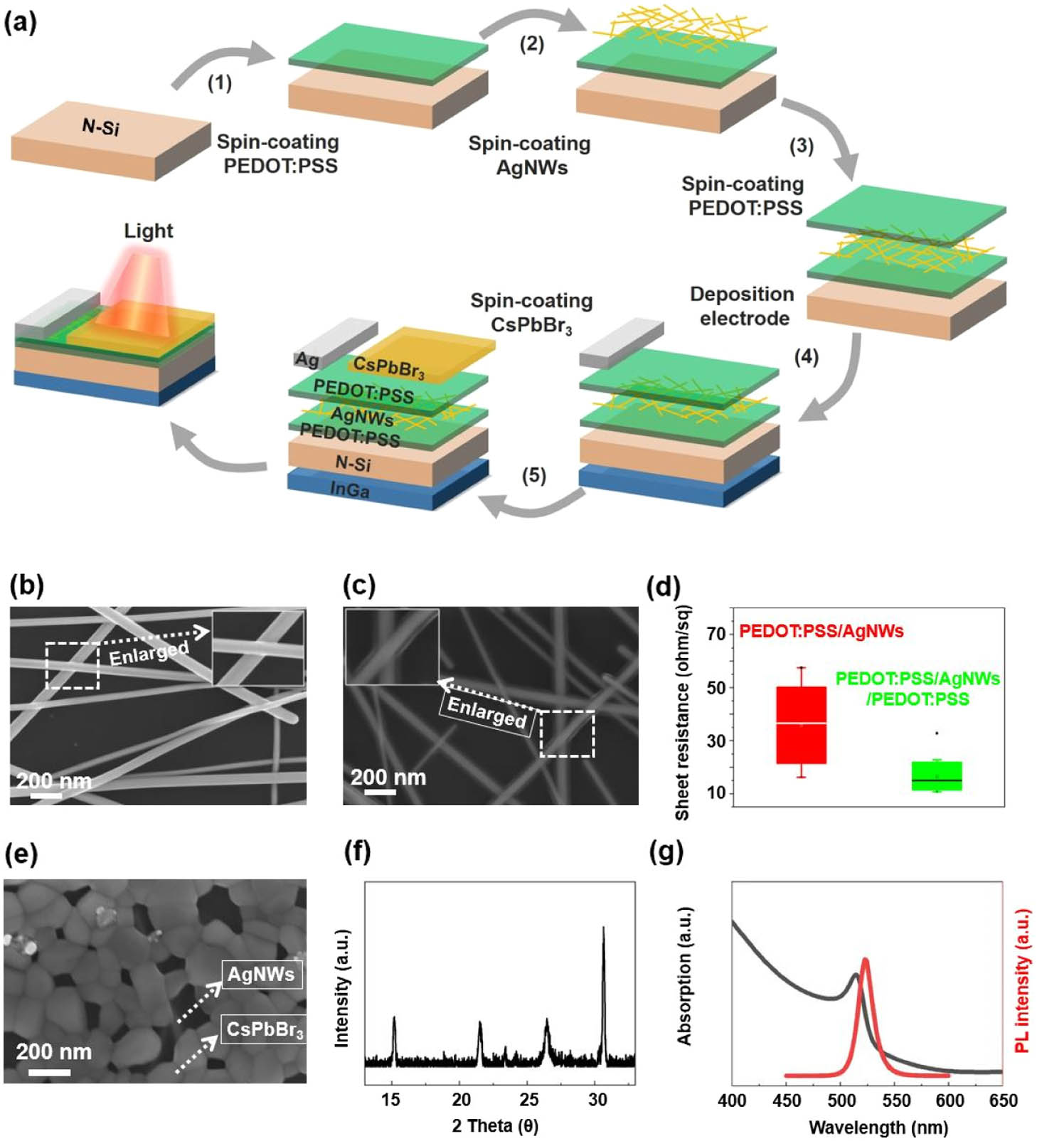
    Figure 1.Fabrication steps of SiCsPbBr3 hybrid PD and materials characterization. (a) Schematic of the fabrication process of the SiCsPbBr3 hybrid PD. (b), (c) Scanning electron microscopy (SEM) images of the PEDOT:PSS/AgNWs (PA) film and PEDOT:PSS/AgNWs/PEDOT:PSS composite layer (PAP-CL), respectively. (d) Sheet resistance of the PA and PAP-CL. (e) Top-view SEM image of the PAP-CL decorated with a CsPbBr3 perovskite layer. (f) X-ray diffraction (XRD) pattern of the CsPbBr3 perovskite film on FTO. (g) Absorbance and photoluminescence (PL) spectra of the CsPbBr3 perovskite film.

    B. Characterization of the Films

    Figures 1(b) and 1(c) show the SEM images of cross-linking AgNWs before and after being covered with the top PEDOT:PSS layer, respectively. The sheet resistance of the PAP-CL is reduced by 2 folds compared with PEDOT:PSS/AgNWs film, as shown in Fig. 1(d). In addition, PAP-CL also exhibits high optical transmittance over 75% in the visible region (Appendix A, Fig. 8). Adjusting the concentration of AgNWs ethanol solution can further adjust the transmission and conductivity of PAP-CL (Appendix A, Fig. 9). Such excellent conductivity and transmittance allow PAP-CL to be used directly as a transparent electrode, which provides an excellent platform for bridging silicon and perovskites. Figure 1(e) shows an SEM image of the PAP-CL covered with CsPbBr3 perovskite. It can be seen that beneath the CsPbBr3 layer are AgNWs, whose structure facilitates carrier transport. We further characterized CsPbBr3 perovskite film. Figure 1(f) shows the XRD pattern of the CsPbBr3 film. The peaks are located at 15.72°, 21.82°, and 30.87°, which correspond to the (100), (110), and (200) crystal planes (PDF#18-0364), respectively. As shown in Fig. 1(g), the absorption spectrum of CsPbBr3 perovskite film exhibits a sharp absorption edge at 540  nm. The steady PL spectrum for the CsPbBr3 perovskite film exhibits a PL peak at 523 nm.

    C. Mechanism Analysis of Spectral Shaping

    In order to reveal the excellent photoresponse performance and flat spectral responsivity in the visible region of the SiCsPbBr3 hybrid PD (device#1), we fabricate three other type devices (device#2–4), as shown in Figs. 2(a)–2(d). First, the CsPbBr3 film is directly spin-coated on the silicon wafer to form the Si/CsPbBr3 heterojunction PD (device#2). This Si/CsPbBr3 PD presents poor photodetection performance, as shown in Fig. 2(e); the enlarged curve is shown in Appendix A, Fig. 10. It is mainly due to the serious interfacial carrier recombination caused by the energy band mismatch between Si and CsPbBr3 [as shown in Fig. 2(j) (device#2)]. Therefore, we introduce a PAP-CL between the Si and CsPbBr3 layers to form the hybrid SiCsPbBr3 PD (device#1) for solving this issue. Thereupon, the responsivity has been significantly improved, benefiting from the formation of Si/PEDOT:PSS heterojunction (device#3), and the shape of spectral responsivity curve in visible region of SiCsPbBr3 hybrid PD is obviously changed compared with the Si/PAP PD as shown in Fig. 2(e). Here, we use a new parameter, F=(MaxMin)/Mean, where Max/Min/Mean, respectively, is the maximum/minimum/mean value in spectral responsivity in the 400–800 nm range, to define “flat.” So, a smaller F value means flatter; further, the F value of device#1/device#3 is 0.6/1.49, indicating the proposed photodetector is flatter than pure silicon photodetectors. From the curve, spectral shaping mainly occurs in two regions (improvement at region I; reduction at region II). Such a spectral shaping changes the linearly reducing tendency in responsivity as the wavelength decreases, and therefore most Si-based PDs obtain a flat spectral responsivity curve in the visible region. The flat spectral responsivity is beneficial to visible HSI. In order to explain the origin of the flat spectral responsivity curve, Fig. 2(f) presents the reflectance spectra of the Si and Si/PAPCL/CsPbBr3 wafers. It can be seen that the intersection of two reflectance spectral curves also forms two differentially behaved regions (I, II), which correspond well with the two regions in Fig. 2(e). It also indicates that the reduction of responsivity in region II is due to the increase of reflectance. Similarly, the reflectance decreases in region I, corresponding to the increase of the spectral responsivity in this region. Obviously, the reduced reflectance implies the enhancement of absorption, which comes from the absorption of CsPbBr3. Then, the key question is whether the photons absorbed by CsPbBr3 contribute to the enhancement of responsivity in region I. In order to clarify this issue, we design device#4 (Si/PAP-CL PD with a glass/CsPbBr3 shielding) and measure its spectral responsivity curve, as shown in Fig. 2(e) (blue line). It can be seen that the responsivity does not improve in region I, implying the CsPbBr3 shielding layer alone is useless for enhancing the performance or shaping the spectral responsivity curve. The above experiment indirectly proves that the PAP-CL can effectively bridge the silicon and CsPbBr3 for a flat spectral responsivity curve. Therefore, introducing a perovskite layer can simultaneously enhance responsivity of the short-wave region due to strong absorption of perovskites and weaken responsivity of the long-wave region due to spectral filtering [Figs. 2(e) and 2(f)]. The proposed photodetector also has the advantage of compactness, i.e., the detector and filter are integrated. Figure 2(g) shows the UPS spectra of CsPbBr3 film on Si or PAP-CL. The UPS spectra of the CsPbBr3 films on a Si wafer or PAP-CL indicate the work function (3.9  eV) of CsPbBr3 perovskite on the n-Si wafer, implying its n-type material. The work function (4.9  eV) of CsPbBr3 on the PAP-CL shows that it becomes a p-type material, which facilitates the holes flowing to CsPbBr3 from the PEDOT:PSS layer (device#1). Finally, Figs. 2(i) and 2(j) show the energy band diagram of device#1, 2, and 3, uncovering the working mechanism of these PDs. In a word, we demonstrate that the spectral responsivity has been shaped to approximately flat by combining CsPbBr3 perovskite to Si-based PD.

    Mechanism analysis of spectrum shaping. (a)–(d) Testing diagrams of Si−CsPbBr3 hybrid PD (device#1), Si/CsPbBr3 PD (device#2), Si/PAP-CL PD (device#3), and Si/PAP PD with a CsPbBr3 shielding layer (device #4), respectively. (e) Spectral responsivity curves (300–1100 nm) of above four devices. (f) Reflectance spectra of Si and Si/PAP-CL/CsPbBr3 wafers. (g), (h) Ultraviolet photoelectron spectroscopy (UPS) spectra of CsPbBr3 on Si or on PAP-CL with the binding energy secondary-electron cutoffs and HOMO regions. (i) Schematic diagram of the energy band alignment of Si, CsPbBr3, and PEDOT:PSS. (j) The corresponding band bending diagram of device#1, 2, and 3.

    Figure 2.Mechanism analysis of spectrum shaping. (a)–(d) Testing diagrams of SiCsPbBr3 hybrid PD (device#1), Si/CsPbBr3 PD (device#2), Si/PAP-CL PD (device#3), and Si/PAP PD with a CsPbBr3 shielding layer (device #4), respectively. (e) Spectral responsivity curves (300–1100 nm) of above four devices. (f) Reflectance spectra of Si and Si/PAP-CL/CsPbBr3 wafers. (g), (h) Ultraviolet photoelectron spectroscopy (UPS) spectra of CsPbBr3 on Si or on PAP-CL with the binding energy secondary-electron cutoffs and HOMO regions. (i) Schematic diagram of the energy band alignment of Si, CsPbBr3, and PEDOT:PSS. (j) The corresponding band bending diagram of device#1, 2, and 3.

    D. Photoresponse Characterization of the SiCsPbBr3 Hybrid PD

    Figure 3(a) shows typical I–V curves of the SiCsPbBr3 hybrid PD illuminated by monochromatic light of 660 nm with different intensity. The active area of the device is 0.125  cm2. It can be seen that the dark current is as low as 2×10⁹  A at zero bias, which means the PD exhibits excellent antinoise ability. Under the light conditions, the results show that the I–V curves of SiCsPbBr3 hybrid PD do not pass the zero point, and the current at zero bias is 106  A, suggesting the device can function in a self-driven mode without an external power supply. Although our device can operate at the zero bias, the external bias voltage can effectively improve the photocurrent to enhance the responsivity of a SiCsPbBr3 hybrid device. Responsivity (R) is defined by R=Iph/Pin=(IlightIdark)/Pin,where Iph, Idark, and Pin are the photocurrent generated under light illumination, dark current, and light power, respectively. As shown in Fig. 3(b), the responsivity curves for the device at different light intensity with different bias can be calculated by the definition. When the incident power is 15 μW (120  μW·cm2 of light intensity), the responsivity at 1 V bias is 0.425A·W1. This SiCsPbBr3 hybrid PD with self-power shows great advantage in simplifying HSI systems; thus, we adopt zero bias in the following experiments.

    Photoresponse characterization of the Si−CsPbBr3 hybrid PD. (a) Current-voltage (I–V) curves of the PD illuminated by 660 nm light with different intensity. (b) The corresponding responsivity at these conditions calculated from (a). (c) Photocurrent intensity as a function of light power under 660 nm light. (d) Photocurrent intensity at weak light region and time-domain dark current curve for calculating noise equivalent power (NEP). (e) Analysis of noise-density spectrum corresponding to time-domain dark current in (d). (f) Calculated detectivity (wavelength of 300–1100 nm) of the PD at different frequency. (g) Transient photovoltage curve for calculating response time. (h) Photovoltage intensity at different light modulation frequency for calculating response bandwidth. (i) Normalized photoresponse of the device for 200 cycles. Top curves are the first and last 10 cycles.

    Figure 3.Photoresponse characterization of the SiCsPbBr3 hybrid PD. (a) Current-voltage (I–V) curves of the PD illuminated by 660 nm light with different intensity. (b) The corresponding responsivity at these conditions calculated from (a). (c) Photocurrent intensity as a function of light power under 660 nm light. (d) Photocurrent intensity at weak light region and time-domain dark current curve for calculating noise equivalent power (NEP). (e) Analysis of noise-density spectrum corresponding to time-domain dark current in (d). (f) Calculated detectivity (wavelength of 300–1100 nm) of the PD at different frequency. (g) Transient photovoltage curve for calculating response time. (h) Photovoltage intensity at different light modulation frequency for calculating response bandwidth. (i) Normalized photoresponse of the device for 200 cycles. Top curves are the first and last 10 cycles.

    Figure 3(c) shows the measured photocurrent intensity with varying incident light power. The results can be well fitted by power law, with an ideal index of 0.93. We further reduce the light power to measure the light current of our PD until the light current is buried in the dark current waveform; therefore, the noise equivalent power (NEP) is calculated as 0.9  nW, as shown in Fig. 3(d).

    To further analyze the noise level of our PD, we measure its detectivity (D*). Here, D* determines the weak-light-signal-detecting ability of a PD, and it comes from NEP: D*=AΔfNEP,where A is the detector area of the active region, and Δf is the working bandwidth (usually set to 1). In this condition, D* is estimated to be 3.9×10⁸ Jones. According to the definition of NEP, D* can be also calculated by D*=RAΔfin,where R is the responsivity and in is the noise current. In many previous reports, researchers often consider shot noise the dominant of noise current, i.e., ignore low-frequency noise. Hence, the calculation of D* can be simplified: D*=RAΔf2qId,where q is the elementary electric charge and Id is the intensity of dark current. In this condition, D* is measured to be 1.4×10¹². However, in imaging applications, researchers often choose to work at a low frequency, even only obtaining a single photocurrent intensity, in order to save imaging time and cost. Therefore, measuring its noise density spectrum and D* at low frequency is necessary. We therefore obtain its noise density spectrum by taking the Fourier transform of the time-domain dark current [42]. The noise current is close to 1010  A·Hz1/2 at 0.01 Hz, which is much higher than that by shot noise (2.68×10¹⁴  A·Hz1/2). Meantime, at high frequency, the noise current gets closer to that by shot noise, which means that our PD not only exists in shot noise but also in some low-frequency noises, e.g., flicker (1/f) noise. We therefore obtain D* at different frequencies (300–1100 nm) according to the calculation method described in Eq. (2), as shown in Fig. 3(f). Relative to the calculation result by simplified method [Eq. (3)], these results are closer to the real values of D* and indicate that our PD has a lower noise level in the visible to infrared region, which benefits the HSI performance in weak light conditions.

    As shown in Fig. 3(g), the rectangular temporal photoresponse curve indicates that our PD has a relatively short rise/fall time (1 ms/2.9 ms), which means it can support fast imaging systems. Meanwhile, we obtain the photovoltage intensity at different light modulation frequencies and calculate a 3  dB response bandwidth (226 Hz), as shown in Fig. 3(h), which is high enough for imaging applications. The photoresponse curves exhibit a similar tendency under periodic light illumination of 200 cycles, as shown in Fig. 3(i). In addition, our device demonstrates over 200-day long-term stability, as shown in Appendix A, Fig. 11. Therefore, it can be concluded that the SiCsPbBr3 hybrid PD is a self-driven and stable perovskite device with high responsivity, low dark current, and a visible-flat spectral responsivity curve.

    4. HYPERSPECTRAL IMAGING DEMONSTRATION

    A. Design of Hyperspectral Imaging System

    To demonstrate the imaging performance of SiCsPbBr3 hybrid PD, we designed an HSI system that combined focused light spatial scanning and monochromatic light spectral scanning. Due to multidimensional scanning, this system is suitable for testing the imaging performance of newly designed, nonarrayed, and unpackaged PDs. Figure 4(a) shows experimental devices used in this paper to realize HSI. A xenon light source emits complex light that includes a 190–2500 nm range. By optical grating, the light becomes monochromatic, whose central wavelength can be controlled by an adjustable slit. Also, the line width can be adjusted to less than 0.1 nm, which ensures spectral resolution of the imaging system. Through the 4f system and focusing lens, the light can be focused into the 100 μm scale, which basically determines the spatial resolution of the imaging system. The imaging sample placed at the focus is driven by a 2D moving platform to realize spatial scanning. In this case, light from the lens can be regarded as incident light (Ii), while diffused reflection light (Idiff) or transmission light (It) can be detected by PD and the subsequent receiving circuit. Depending on the type of light received, the PD needs to be placed in different positions [R PD or T PD in Fig. 4(a)]; thereupon, reflection mode or transmission mode imaging can be realized. Furthermore, absorption imaging is possible when scattered light is collected in all directions because absorbed light (Ia) equals incident light (Ii) subtracting diffused light (Idiff) and transmission light (It). Figure 4(b) shows the data analysis method in HSI. By spatial scanning and spectral scanning, a hyperspectral data cube C(x,y,λ) is obtained, which can be presented as images (x, y) at multiple wavelengths (λ). Generally speaking, the cube needs at least several dozen wavelengths (N) in the spectral dimension. Relative spectrum at a certain position (x0,y0) can be obtained by curving the value of the same pixel (x0,y0) in images at different wavelengths (λ), i.e., spectrum (x0,y0)=I(x,y,λ)|(x=x0,y=y0). After calibration by standard sample, an accurate spectrum can be obtained. In particular, transmissivity [T(x,y)] equals the quotient of transmission light intensity (It) and incident light intensity (Ii), while relative reflectivity [R(x,y)] equals the quotient of diffused light (Idiff) and diffused light of standard white plate (Id). The spatial arrangement of the filters is shown in Appendix A, Fig. 12 and Fig. 13. From as-displayed images at multiple wavelengths, it can be seen that only when the wavelength matches, the image will be a bright color. Further, transmissivity spectra obtained by the above-mentioned method have sharp peaks, which agree well with the values measured by a spectrophotometer. It can be concluded that the method presented in this paper is feasible and demonstrates potential in biomedical imaging.

    Schematic diagram of our hyperspectral imaging system. (a) Experimental devices used in this paper to realize hyperspectral imaging. R/T PD: PD for reflection/transmission mode imaging. (b) Data analysis in our hyperspectral imaging system, where k (k=1−N) represents spectral (λ) ordinal and (i, j) represent spatial (x, y) ordinals.

    Figure 4.Schematic diagram of our hyperspectral imaging system. (a) Experimental devices used in this paper to realize hyperspectral imaging. R/T PD: PD for reflection/transmission mode imaging. (b) Data analysis in our hyperspectral imaging system, where k (k=1N) represents spectral (λ) ordinal and (i, j) represent spatial (x, y) ordinals.

    Multispectral imaging results of the Si-PD and Si−CsPbBr3 PD proposed in this work when in strong and weak light. Note that the light intensity is measured from the incident light; there also may be differences of the diffuse light reaching the PDs when changing PDs.

    Figure 5.Multispectral imaging results of the Si-PD and SiCsPbBr3 PD proposed in this work when in strong and weak light. Note that the light intensity is measured from the incident light; there also may be differences of the diffuse light reaching the PDs when changing PDs.

    Reflectance mode hyperspectral imaging for tumor detection. (a) Images of resected tissue at multiple wavelengths. (b) Photographs of tumor-bearing mouse and fresh resected tissue. (c) Calculated reflection spectra from our hyperspectral imaging system. (d) The spectrum measured by conventional spectrophotometer with no spatial resolution.

    Figure 6.Reflectance mode hyperspectral imaging for tumor detection. (a) Images of resected tissue at multiple wavelengths. (b) Photographs of tumor-bearing mouse and fresh resected tissue. (c) Calculated reflection spectra from our hyperspectral imaging system. (d) The spectrum measured by conventional spectrophotometer with no spatial resolution.

    B. Multispectral Imaging Results of the Si-PD and SiCsPbBr3 PD

    As we know, responsivity of photodetectors (PDs) is a key parameter for evaluating photosensitive ability. Conventional Si-based PDs exhibit poor responsivity at short wavelengths (e.g,. 400–600 nm) compared with that at a longer wavelength region due to the nature of the indirect bandgap in silicon of around 1.1 eV, which indicates the conventional Si-based PDs have poorer performance at 400–600 nm, as shown in Fig. 5. More obviously, such cases will happen when the illumination light is weak, as shown in Fig. 5(b). Therefore, improvements of the responsivity at 400–600 nm are important for enhancing the HSI quality at 400–600 nm.

    C. Reflectance Mode Hyperspectral Imaging for Tumor Detection

    Tumor detection and identification are major challenges in the biomedical field. Despite having a high blood supply, most tumors suffer from hypoxia because of tortuous vessels and high metabolism. One consequence is that hemoglobin concentration in the tumor region is significantly higher than normal tissue. Also, the proportion of deoxygenated hemoglobin becomes higher. In a spectrum, a tumor shows more absorption and less reflection in the 500–600 nm range. Therefore, HSI provides us with a new probability to detect a tumor. Figure 6 provides an example to demonstrate HSI for tumor detection. Figure 6(a) shows images of resected tissue at multiple wavelengths from 400 to 790 nm. Visually, the profile of tissue of images at 500–790 nm is consistent with the photograph [Fig. 6(b)] of fresh resected tissue, but the profile at 400–490 nm is ambiguous. That may be led by the color of hemoglobin, which is predominant in biological tissues. For more accurate analysis, we randomly select two pixels in the tumor region (A and B) and two in the normal region (C and D). The reflection spectra from HSI in Fig. 6(c) are calculated by the method described in Fig. 4. From the spectra, it is obvious that reflectivity in the tumor region is significantly less than that in the normal region in the 500–790 nm range. Further, the spectra of pixels A, B, C, and D have certain similarity with ill-informed spectrum measured by a spectrophotometer, which is shown in Fig. 6(d). Here, the spectrum is captured approximately in the middle of the tissue. This spectrum is obtained by a UV-vis spectrophotometer (Shimadzu, UV-2600), whose working light has a light spot with a size of 5  mm×15  mm. Thus, the spectrum can be regarded as the average value in the light spot, meaning this spectrum has no spatial information. It is indicated that a hyperspectral data cube C(x,y,λ) has abundant spatial and spectral information compared with a 2D image alone and a spectral curve alone. Then, a proper classification algorithm may help to differentiate tumor tissues [43].

    D. Transmission Mode Hyperspectral Imaging for Tissue Identification

    Biological tissue usually has its own unique color due to difference of type and content of color molecules. For example, liver is rich in blood so that it shows dark red, while a neighboring cholecyst is green due to bile. In addition to endogenous color, tissue section usually is stained in order to increase contrast. Considering that HSI contains spatial and spectral information, it is suitable for tissue identification. Figures 7(a) and 7(b) show transmission images of myocardium and liver sections at multiple wavelengths, respectively. Corresponding photographs of tissue sections are shown in Fig. 7(c). Using a similar data-processing method as that in Figs. 4 and 6, transmission spectra can be extracted from the images, as shown in Fig. 7(d). From the results, HSI can obtain spatial information corresponding to a photograph and spectral information corresponding to a spectrogram. Based on the obtained spatial and spectral information, a classification methodology can be used for tissue identification.

    Transmission mode hyperspectral imaging for tissue identification. (a) Images of myocardium section at multiple wavelengths. (b) Images of liver section at multiple wavelengths. (c) Photographs of the tissue sections. (d) Corresponding transmission spectra measured by conventional spectrophotometer and our hyperspectral imaging system.

    Figure 7.Transmission mode hyperspectral imaging for tissue identification. (a) Images of myocardium section at multiple wavelengths. (b) Images of liver section at multiple wavelengths. (c) Photographs of the tissue sections. (d) Corresponding transmission spectra measured by conventional spectrophotometer and our hyperspectral imaging system.

    5. DISCUSSION

    By performing point scanning in this paper, theoretically, the pose (direction/position) of the output beam would be different for different wavelengths. Therefore, the output beam might not be equally past the pinhole (due to off-axis aberration) and also cause displacement of the sample surface. However, it does not show up on current imaging results due to big scanning steps and low resolution. The issue may be serious in microscopy imaging. Further, point scanning is time-consuming compared with other methods. The total imaging time to obtain an HSI data cube depends on step distance, number of steps, number of spectra, and so on. Typically, obtaining images shown in Fig. 5 costs 20  min. An HSI system adopting pushbroom, staring, or snapshot requires 2D array detectors with megapixels or 1D array detectors with thousands of pixels. However, this paper means to solve the spectral responsivity issue, so the detector with only one pixel was made (how to make an array detector is an engineering issue not covered in this paper). In order to show the imaging performance of the proposed HSI detector, a scanning system was used here. Fortunately, the proposed Si-based photodetector is compatible with the mature silicon fabrication processes; thus, once the array detectors are created, the HSI system combined with other scanning methods (e.g.,  pushbroom, staring, snapshot HSI) and the proposed HSI detector may demonstrate better performance than that of existing HSI systems.

    As for the cost, we believe the proposed photodetector is not with high cost, because the proposed Si-based photodetector is easily compatible with mature silicon fabrication processes. Compared with a pure silicon detector, the additional process is only the spin-coating of perovskites and PEDOT:PSS/AgNWs, which are low-cost materials. Therefore, once mass-produced, the cost of the proposed detector will not be too high.

    In this paper, we use light splitting combined with a broadband photodetector to obtain spectral resolution. Alternatively, a set of narrowband photodetectors illuminated by ambient light or natural light may be more convenient for HSI. However, the narrowband photodetectors may have reduced and unflat responsivity [44]. Also, these nonsilicon detectors may not be compatible with the mature silicon fabrication processes, thus causing an array issue. Therefore, narrowband photodetector-based HSI still has a long way to go.

    6. CONCLUSIONS

    In this paper, we fabricate a novel SiCsPbBr3 hybrid PD possessing the flat spectral responsivity in the visible region. Further, we demonstrate a SiCsPbBr3 hybrid PD-based HSI system for tumor detection and tissue identification. We believe that this SiCsPbBr3 hybrid PD is a milestone for low-cost, broadband, and high-performance HSI, with broad potential applications in bioimaging.

    Acknowledgment

    Acknowledgment. H. F. thanks the financial support from Agency for Science, Technology, and Research (A*STAR), Singapore by AME Individual Research.

    APPENDIX A

    The transmittance spectra of FTO, FTO/AgNWs/PEDOT:PSS and FTO/TO/AgNWs/PEDOT:PSS/AgNWs/PEDOT:PSS films.

    Figure 8.The transmittance spectra of FTO, FTO/AgNWs/PEDOT:PSS and FTO/TO/AgNWs/PEDOT:PSS/AgNWs/PEDOT:PSS films.

    Scanning electron microscopy (SEM) images of the PEDOT:PSS/AgNWs/ PEDOT:PSS composite films with different concentration of AgNWs ethanol solution.

    Figure 9.Scanning electron microscopy (SEM) images of the PEDOT:PSS/AgNWs/ PEDOT:PSS composite films with different concentration of AgNWs ethanol solution.

    (a) Spectral response curve of the Si/CsPbBr3 device. (b) Energy band diagram of the Si/CsPbBr3 PD.

    Figure 10.(a) Spectral response curve of the Si/CsPbBr3 device. (b) Energy band diagram of the Si/CsPbBr3 PD.

    Long-term stability of the Si−CsPbBr3 hybrid device.

    Figure 11.Long-term stability of the SiCsPbBr3 hybrid device.

    (a) Data cube with bandpass light filter as the imaging object. (b) Transmittivity comparison of calculated values by hyperspectral imaging and measured values by spectrophotometer.

    Figure 12.(a) Data cube with bandpass light filter as the imaging object. (b) Transmittivity comparison of calculated values by hyperspectral imaging and measured values by spectrophotometer.

    Detail images in the experiment of Fig. 12.

    Figure 13.Detail images in the experiment of Fig. 12.

    References

    [1] D. Bannon. Cubes and slices. Nat. Photonics, 3, 627-629(2009).

    [2] G. Lu, B. Fei. Medical hyperspectral imaging: a review. J. Biomed. Opt., 19, 010901(2014).

    [3] F. Yesilkoy, E. R. Arvelo, Y. Jahani, M. Liu, A. Tittl, V. Cevher, Y. Kivshar, H. Altug. Ultrasensitive hyperspectral imaging and biodetection enabled by dielectric metasurfaces. Nat. Photonics, 13, 390-396(2019).

    [4] L. Gevaux, C. Adnet, P. Seroul, R. Clerc, A. Tremeau, J. L. Perrot, M. Hebert. Three-dimensional maps of human skin properties on full face with shadows using 3-D hyperspectral imaging. J. Biomed. Opt., 24, 066002(2019).

    [5] D. T. Dicker, J. Lerner, P. Van Belle, S. F. Barth, D. T. Guerry, M. Herlyn, D. E. Elder, W. S. El-Deiry. Differentiation of normal skin and melanoma using high resolution hyperspectral imaging. Cancer Biol. Ther., 5, 1033-1038(2006).

    [6] M. Halicek, H. Fabelo, S. Ortega, G. M. Callico, B. Fei. In-vivo and ex-vivo tissue analysis through hyperspectral imaging techniques: revealing the invisible features of cancer. Cancers, 11, 756(2019).

    [7] H. Akbari, K. Uto, Y. Kosugi, K. Kojima, N. Tanaka. Cancer detection using infrared hyperspectral imaging. Cancer Sci., 102, 852-857(2011).

    [8] Z. Liu, H. Wang, Q. Li. Tongue tumor detection in medical hyperspectral images. Sensors, 12, 162-174(2012).

    [9] J. Yoon, J. Joseph, D. J. Waterhouse, A. S. Luthman, G. S. D. Gordon, M. Di Pietro, W. Januszewicz, R. C. Fitzgerald, S. E. Bohndiek. A clinically translatable hyperspectral endoscopy (HySE) system for imaging the gastrointestinal tract. Nat. Commun., 10, 1902(2019).

    [10] X. Hadoux, F. Hui, J. K. H. Lim, C. L. Masters, A. Pebay, S. Chevalier, J. Ha, S. Loi, C. J. Fowler, C. Rowe, V. L. Villemagne, E. N. Taylor, C. Fluke, J. P. Soucy, F. Lesage, J. P. Sylvestre, P. Rosa-Neto, S. Mathotaarachchi, S. Gauthier, Z. S. Nasreddine, J. D. Arbour, M. A. Rheaume, S. Beaulieu, M. Dirani, C. T. O. Nguyen, B. V. Bui, R. Williamson, J. G. Crowston, P. Van Wijngaarden. Non-invasive in vivo hyperspectral imaging of the retina for potential biomarker use in Alzheimer’s disease. Nat. Commun., 10, 4227(2019).

    [11] R. L. Greenman, S. Panasyuk, X. Wang, T. E. Lyons, T. Dinh, L. Longoria, J. M. Giurini, J. Freeman, L. Khaodhiar, A. Veves. Early changes in the skin microcirculation and muscle metabolism of the diabetic foot. Lancet, 366, 1711-1717(2005).

    [12] M. E. M. Seong, G. Kong, T. Vo-Dinh. Hyperspectral fluorescence imaging for mouse skin tumor detection. ETRI J., 28, 770-776(2006).

    [13] D. Yudovsky, A. Nouvong, K. Schomacker, L. Pilon. Assessing diabetic foot ulcer development risk with hyperspectral tissue oximetry. J. Biomed. Opt., 16, 026009(2011).

    [14] J. K. Muhammad, S. K. Hamid, Y. Adeel, K. Khurram, A. Abbas. Modern trends in hyperspectral image analysis: a review. IEEE Access, 6, 14118-14129(2018).

    [15] I. Amenabar, S. Poly, M. Goikoetxea, W. Nuansing, P. Lasch, R. Hillenbrand. Hyperspectral infrared nanoimaging of organic samples based on Fourier transform infrared nanospectroscopy. Nat. Commun., 8, 14402(2017).

    [16] S. Kumar, C. Desmedt, D. Larsimont, C. Sotiriou, E. Goormaghtigh. Change in the microenvironment of breast cancer studied by FTIR imaging. Analyst, 138, 4058-4065(2013).

    [17] E. L. Larsen, L. L. Randeberg, E. Olstad, O. A. Haugen, A. Aksnes, L. O. Svaasand. Hyperspectral imaging of atherosclerotic plaques in vitro. J. Biomed. Opt., 16, 026011(2011).

    [18] B. S. Sorg, B. J. Moeller, O. Donovan, Y. Cao, M. W. Dewhirst. Hyperspectral imaging of hemoglobin saturation in tumor microvasculature and tumor hypoxia development. J. Biomed. Opt., 10, 44004(2005).

    [19] V. Tuchin. Tissue optics and photonics: light-tissue interaction II. J. Biomed. Photon. Eng., 2, 030201(2016).

    [20] K. Mangold, J. A. Shaw, M. Vollmer. The physics of near-infrared photography. Eur. J. Phys., 34, S51-S71(2013).

    [21] Y. Liu, J. Zhu, G. Cen, J. Zheng, D. Xie, Z. Zhao, C. Zhao, W. Mai. Valence-state controllable fabrication of Cu2-xO/Si type-II heterojunction for high-performance photodetectors. ACS Appl. Mater. Interfaces, 11, 43376-43382(2019).

    [22] Y. Liu, G. Cen, G. Wang, J. Huang, S. Zhou, J. Zheng, Y. Fu, C. Zhao, W. Mai. High performance MoO3−x/Si heterojunction photodetectors with nanoporous pyramid Si arrays for visible light communication application. J. Mater. Chem. C, 7, 917-925(2019).

    [23] Y. Zhang, Y. Yu, L. Mi, H. Wang, Z. Zhu, Q. Wu, Y. Zhang, Y. Jiang. In situ fabrication of vertical multilayered MoS2/Si homotype heterojunction for high-speed visible-near-infrared photodetectors. Small, 12, 1062-1071(2016).

    [24] Z. Ji, Y. Liu, W. Li, C. Zhao, W. Mai. Reducing current fluctuation of Cs3Bi2Br9 perovskite photodetectors for diffuse reflection imaging with wide dynamic range. Sci. Bull., 65, 1371-1379(2020).

    [25] K. Leng, I. Abdelwahab, I. Verzhbitskiy, M. Telychko, L. Chu, W. Fu, X. Chi, N. Guo, Z. Chen, Z. Chen, C. Zhang, Q. H. Xu, J. Lu, M. Chhowalla, G. Eda, K. P. Loh. Molecularly thin two-dimensional hybrid perovskites with tunable optoelectronic properties due to reversible surface relaxation. Nat. Mater., 17, 908-914(2018).

    [26] F. P. G. De Arquer, A. Armin, P. Meredith, E. H. Sargent. Solution-processed semiconductors for next-generation photodetectors. Nat. Rev. Mater., 2, 16100(2017).

    [27] F. Li, C. Ma, H. Wang, W. Hu, W. Yu, A. D. Sheikh, T. Wu. Ambipolar solution-processed hybrid perovskite phototransistors. Nat. Commun., 6, 8238(2015).

    [28] Q. Chen, J. Wu, X. Ou, B. Huang, J. Almutlaq, A. A. Zhumekenov, X. Guan, S. Han, L. Liang, Z. Yi, J. Li, X. Xie, Y. Wang, Y. Li, D. Fan, D. B. L. Teh, A. H. All, O. F. Mohammed, O. M. Bakr, T. Wu, M. Bettinelli, H. Yang, W. Huang, X. Liu. All-inorganic perovskite nanocrystal scintillators. Nature, 561, 88-93(2018).

    [29] L. Dou, Y. M. Yang, J. You, Z. Hong, W. H. Chang, G. Li, Y. Yang. Solution-processed hybrid perovskite photodetectors with high detectivity. Nat. Commun., 5, 5404(2014).

    [30] Z. Ji, Y. Liu, W. Mai. Enhancing the photodetection performance of MAPbI3 perovskite photodetectors by a dual functional interfacial layer for color imaging. Opt. Lett., 46, 150-153(2021).

    [31] G. Cen, Y. Liu, C. Zhao, G. Wang, Y. Fu, G. Yan, Y. Yuan, C. Su, Z. Zhao, W. Mai. Atomic-layer deposition-assisted double-side interfacial engineering for high-performance flexible and stable CsPbBr3 perovskite photodetectors toward visible light communication applications. Small, 15, 1902135(2019).

    [32] Y. Fu, H. Zhu, J. Chen, M. P. Hautzinger, X. Y. Zhu, S. Jin. Metal halide perovskite nanostructures for optoelectronic applications and the study of physical properties. Nat. Rev. Mater., 4, 169-188(2019).

    [33] V. V. Belykh, D. R. Yakovlev, M. M. Glazov, P. S. Grigoryev, M. Hussain, J. Rautert, D. N. Dirin, M. V. Kovalenko, M. Bayer. Coherent spin dynamics of electrons and holes in CsPbBr3 perovskite crystals. Nat. Commun., 10, 673(2019).

    [34] A. P. Schlaus, M. S. Spencer, K. Miyata, F. Liu, X. Wang, I. Datta, M. Lipson, A. Pan, X. Y. Zhu. How lasing happens in CsPbBr3 perovskite nanowires. Nat. Commun., 10, 265(2019).

    [35] A. Manzi, Y. Tong, J. Feucht, E. P. Yao, L. Polavarapu, A. S. Urban, J. Feldmann. Resonantly enhanced multiple exciton generation through below-band-gap multi-photon absorption in perovskite nanocrystals. Nat. Commun., 9, 1518(2018).

    [36] Z. Ji, G. Cen, C. Su, Y. Liu, Z. Zhao, C. Zhao, W. Mai. All-inorganic perovskite photodetectors with ultrabroad linear dynamic range for weak-light imaging applications. Adv. Opt. Mater., 8, 2001436(2020).

    [37] F. Sahli, J. Werner, B. A. Kamino, M. Bräuninger, R. Monnard, B. Paviet-Salomon, L. Barraud, L. Ding, J. J. D. Leon, D. Sacchetto, G. Cattaneo, M. Despeisse, M. Boccard, S. Nicolay, Q. Jeangros, B. Niesen, C. Ballif. Fully textured monolithic perovskite/silicon tandem solar cells with 25.2% power conversion efficiency. Nat. Mater., 17, 820-826(2018).

    [38] T. Leijtens, K. A. Bush, R. Prasanna, M. D. McGehee. Opportunities and challenges for tandem solar cells using metal halide perovskite semiconductors. Nat. Energy, 3, 828-838(2018).

    [39] Z. Liang, P. Zeng, P. Liu, C. Zhao, W. Xie, W. Mai. Interface engineering to boost photoresponse performance of self-powered, broad-bandwidth PEDOT:PSS/Si heterojunction photodetector. ACS Appl. Mater. Inter., 8, 19158-19167(2016).

    [40] J. P. Thomas, M. A. Rahman, S. Srivastava, J. S. Kang, D. Mcgillivray, M. Abd-Ellah, N. F. Heinig, K. T. Leung. Highly conducting hybrid silver-nanowire-embedded poly(3,4-ethylenedioxythiophene): poly (styrene sulfonate) for high-efficiency planar silicon/organic heterojunction solar cells. ACS Nano, 12, 9495-9503(2018).

    [41] R. Shimotsu, T. Takumi, V. Vohra. All solution-processed micro-structured flexible electrodes for low-cost light-emitting pressure sensors fabrication. Sci. Rep., 7, 6921(2017).

    [42] C. H. Liu, Y. C. Chang, T. B. Norris, Z. Zhong. Graphene photodetectors with ultra-broadband and high responsivity at room temperature. Nat. Nanotechnol., 9, 273-278(2014).

    [43] H. Abbasi, G. Rauter, R. Guzman, P. C. Cattin, A. Zam. Differentiation of femur bone from surrounding soft tissue using laser-induced breakdown spectroscopy as a feedback system for smart laserosteotomy. Proc. SPIE, 10685, 1068519(2018).

    [44] Y. Fang, Q. Dong, Y. Shao, Y. Yuan, J. Huang. Highly narrowband perovskite single-crystal photodetectors enabled by surface-charge recombination. Nat. Photonics, 9, 679-686(2015).

    Yujin Liu, Zhong Ji, Yaping Li, Hong Jin Fan, Wenjie Mai. Spectrum-shaped Si-perovskite hybrid photodetectors for hyperspectral bioimaging[J]. Photonics Research, 2021, 9(9): 1734
    Download Citation