Beijing National Research Center for Information Science and Technology, Department of Electronic Engineering, Tsinghua University, Beijing 100084, China
Ever-growing deep-learning technologies are making revolutionary changes for modern life. However, conventional computing architectures are designed to process sequential and digital programs but are burdened with performing massive parallel and adaptive deep-learning applications. Photonic integrated circuits provide an efficient approach to mitigate bandwidth limitations and the power-wall brought on by its electronic counterparts, showing great potential in ultrafast and energy-free high-performance computation. Here, we propose an optical computing architecture enabled by on-chip diffraction to implement convolutional acceleration, termed “optical convolution unit” (OCU). We demonstrate that any real-valued convolution kernels can be exploited by the OCU with a prominent computational throughput boosting via the concept of structral reparameterization. With the OCU as the fundamental unit, we build an optical convolutional neural network (oCNN) to implement two popular deep learning tasks: classification and regression. For classification, Fashion Modified National Institute of Standards and Technology (Fashion-MNIST) and Canadian Institute for Advanced Research (CIFAR-4) data sets are tested with accuracies of 91.63% and 86.25%, respectively. For regression, we build an optical denoising convolutional neural network to handle Gaussian noise in gray-scale images with noise level , 15, and 20, resulting in clean images with an average peak signal-to-noise ratio (PSNR) of 31.70, 29.39, and 27.72 dB, respectively. The proposed OCU presents remarkable performance of low energy consumption and high information density due to its fully passive nature and compact footprint, providing a parallel while lightweight solution for future compute-in-memory architecture to handle high dimensional tensors in deep learning.
1. INTRODUCTION
Convolutional neural networks (CNNs) [1–3] power enormous applications in the artificial intelligence (AI) world, including computer vision [4–6], self-driving cars [7–9], natural language processing [10–12], medical science [13–15], etc. Inspired by biological behaviors of visual cortex systems, CNNs have brought remarkable breakthroughs in manipulating high-dimensional tensor such as images, videos, and speech, enabling efficient processing with more precise information extractions but much fewer network parameters, compared with the classical feed-forward one. However, advanced CNN algorithms have rigorous requirements on computing platforms, which are responsible for massive data throughputs and computations, which have triggered the flourishing development of high-performance computing hardware such as the central processing unit [16], graphics processing unit [17], tensor processing unit (TPU) [18], and field-programmable gate array [19]. Nonetheless, today’s electronic computing architectures are facing physical bottlenecks in processing distribution and parallel tensor operations, e.g., bandwidth limitation, high-power consumption, and the fading of Moore’s law, causing serious computation force mismatches between AI and the underlying hardware frameworks.
Important progress has been made to further improve the capabilities of future computing hardware. In recent years, the optical neural network (ONN) [20–27] has received growing attention with its extraordinary performance in facilitating complex neuromorphic computations. The intrinsic parallelism nature of optics enables more than 10 THz interconnection bandwidth [28], and the analog fashion of photonics system [29] decouplings demonstrates the urgent need for high-performance memory in conventional electronic architectures and therefore prevents energy wasting and time latency from continuous AD/DA conversion and arithmetic logic unit (ALU)-memory communication, thus boosting computational speed and reducing power consumption essentially.
To date, numerous ONNs have been proposed to apply various neuromorphic computations such as optical inference networks based on Mach–Zehnder interferometer (MZI) mesh [30–32], photonics spiking neural networks based on an wavelength division multiplexing (WDM) protocol and ring modulator array [33–35], photonics tensor core based on phase change materials [36,37], and optical accelerator based on time-wavelength interleaving [38–40]. For higher computation capabilities of ONNs, diffractive optical neural networks [41–44] have been proposed to provide millions of trainable connections and neurons optically by means of light diffraction. To further improve network density, the integrated fashion of diffractive optical neural networks based on an optical discrete Fourier transform [45], multimode interference [46], and metasurface technologies [47–49] has been studied. However, these on-chip diffraction approaches are limited by power consumption and input dimensions, making them difficult to scale up for adapting massive parallel high-order tensor computations. Here, we take one step forward to address this issue by building an optical convolution unit (OCU) with on-chip optical diffraction and cascaded 1D metalines on a standard silicon on insulator (SOI) platform. We demonstrate that any real-valued convolution kernels can be exploited by an OCU with a prominent computation power. Furthermore, with the OCU as the basic building block, we build an optical convolutional neural network (oCNN) to perform classification and regression tasks. For classification tasks, Fashion-MNIST and CIFAR-4 data sets are tested with accuracies of 91.63% and 86.25%, respectively. For regression tasks, we build an optical denoising convolutional neural network (oDnCNN) to handle Gaussian noise in gray-scale images with noise level , 15, and 20, resulting in clean images with average peak signal-to-noise ratio (PSNR) of 31.70, 29.39, and 27.72 dB. The proposed OCU and oCNN are fully passive in processing massive tensor data and compatible for ultrahigh bandwidth interfaces (for both electronic and optical), being capable of integrating with electronic processors to reaggregate computational resources and power penalties.
Sign up for Photonics Research TOC. Get the latest issue of Photonics Research delivered right to you!Sign up now
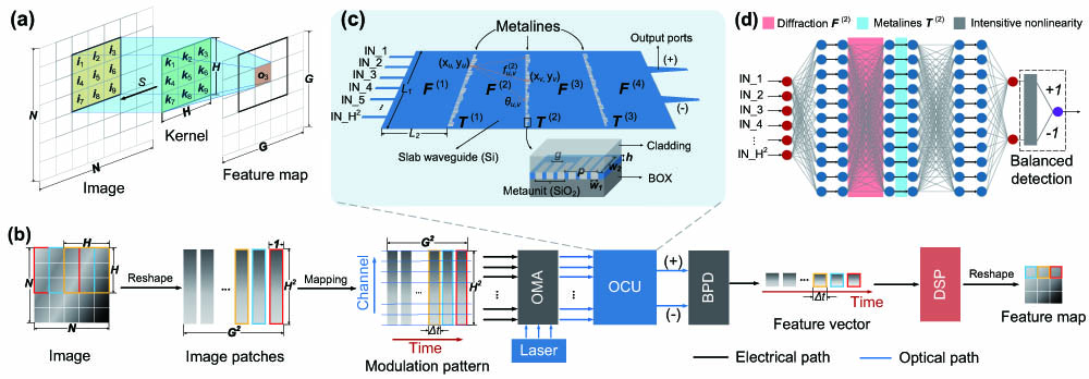
2. PRINCIPLE
Figure 1(a) presents the operation principle of 2D convolution. Here, a fixed kernel with size of slides over the image with size of by stride of and does weighted addition with the image patches that are covered by the kernel, resulting an extracted feature map with size of , where (in this case, we ignore the padding process of convolution). This process can be expressed in Eq. (1), where represents a pixel of the feature map, and and are related to the stride . Based on this, one can simplify the operation as multiplications between an vector reshaped by the kernel and a matrix composed by image patches, as shown in Eq. (2): where , and is a corresponding image patch covered by a sliding kernel, and denotes the flattened feature vector. Consequently, the fundamental idea of optical 2D convolution is to manipulate multiple vector-vector multiplications optically and keep their products in series for reshaping to a new map. Here, we use on-chip optical diffraction to implement this process, as described in Fig. 1(b). The input image with size of is first reshaped into flattened patches according to the kernel size and sliding stride , which turns the image into a matrix . Then, is mapped into a plane of space channels and time, in which each row of is varied temporarily with period of and each column of (namely, pixels of a flattened image patch) is distributed in channels. A coherent laser signal is split into paths and then modulated individually by the time-encoded and channel-distributed image patches, in either amplitude or phase. In this way, one time slot with duration of contains one image patch with pixels in corresponding channels, and of these time slots can fully express image patch matrix . Then, the coded light is sent to the proposed OCU to perform matrix multiplications as Eq. (2) shows, and the corresponding positive and negative results are detected by a balanced photodetector (BPD) to do subtractions between the two. The balanced detection scheme assures the OCU operates in a real-valued field. The detected information is varied temporarily with symbol duration of and then reshaped into a new feature map by a digital signal processor (DSP). The principle is also applicable for images and kernels that have nonsquare shapes.
Figure 1.Principle of optical image convolution based on OCU. (a) Operation principle of 2D convolution. A fixed kernel with size of slides over the image with size of by stride of and does weighted addition with the image patches that are covered by the kernel, resulting in an extracted feature map with size of , where . (b) Optical image convolution architecture with OCU. An image is first flattened into patches according to the kernel size and sliding stride and then mapped into a modulation pattern confined with time and channel number, which modulates a coherent laser via a modulation array. The modulated light is sent to OCU to perform optical convolution, whose positive and negative results are subtracted by a balanced photodetector and reshaped by a DSP to form a new feature map. OMA, optical modulator array; BPD, balanced photodetector; DSP, digital signal processor. (c) Details of OCU. waveguides are used to send a laser signal into a silicon slab waveguide with size of , and layers of metaline are exploited successively with layer gap of , which are composed by well-arranged metaunits. Three identical silica slots with sizes of are used to compose one metaunit with gap of , and the period of metaunits is . The phase modulation is implemented by varying . The transfer function of the diffraction in slab waveguide and phase modulation of metalines are denoted as and . (d) The feedforward neural network abstracted from the OCU model. Red and blue boxes denote diffractions and phase modulations of metalines; gray box represents intensitive nonlinear activation of complex-valued neural networks introduced by photodetection.
The details of OCU are given in Fig. 1(c). Here, silicon strip waveguides are exploited for receiving signals simultaneously from modulation channels, which diffract and interfere with each other in a silicon slab waveguide with size of before it encounters well-designed 1D metalines. The 1D metaline is a subwavelength grating consisting of silica slots with each slot having a size of , which is illustrated in the inset of Fig. 1(c). Furthermore, we use three identical slots with slot gap of to constitute a metaunit with period of to ensure a constant effective refractive index of the 1D metaline when it meets light from different angles, as demonstrated in our previous work [48,49]. The incoming signal is phase-modulated from 0 to by changing the length of each metaunit but with and fixed. Accordingly, the corresponding length of the th metaunit in the th metaline can be ascertained from the introduced phase delay by Eq. (3), where and are the effective refractive index of the slab and slots, respectively. After layers of propagation, the interfered light is sent to two ports, which output positive and negative part of computing results
For more precise analysis, the diffraction in the slab waveguide between two metalines with and metaunits, respectively, is characterized by a matrix based on the Huygens–Fresnel principle under restricted propagation conditions, whose element , as shown in Eq. (4), is the diffractive connection between the th metaunit located at of the ()th metaline, and the th metaunit locates at in the th metaline, cos , denotes the distance between the two metaunits, is working wavelength, is the imaginary unit, and and are the amplitude and phase coefficients, respectively. As for each metaline, the introduced phase modulation is modeled by a diagonal matrix , as expressed in Eq. (5):
To prove the accuracy of the proposed model in Eqs. (4) and (5), we evaluate the optical field of an OCU with finite-different time-domain (FDTD) method, as shown in Fig. 2(a). Three metalines with 10 metaunits for each are configured based on a standard SOI platform, the size of slab waveguide between the metalines is μμ, the width and gap of slots are set to be 200 and 500 nm, the period of metaunit is 1.5 μm, and a laser source is split to nine waveguides with working wavelength of 1550 nm. We monitor the amplitude and phase response of the diffracted optical field at Position A of Fig. 2(a), which agree well with the proposed analytical model in Eq. (4), as shown in Figs. 2(b) and 2(c). Phase modulation of the metaline is also validated by monitoring the optical phase response at Position B in Fig. 2(d), with the incident light of a plane wave. Figure 2(e) shows an ideal match between the FDTD calculation and the analytical model in Eq. (5).
Figure 2.(a) Optical field of the OCU evaluated by FDTD method. A monitor is set at Position A to receive the optical field of the incident light. (b) Magnitude and (c) phase response of the optical field at Position A (red solid curve) match well with the analytical model (purple dash curve) in Eq. (5). (d) Optical field of the metaline with incident light of a plane wave. A monitor is set behind the metaline at Position B to obtain its phase response. (e) The analytical model (purple dash curve) of Eq. (6) fits well with the FDTD calculation (red solid curve).
Consequently, we conclude the OCU model in Eq. (6), where is the layer number of OCU and is the response of the OCU when the input is a reshaped image patch matrix . Besides, the numbers of metaunits in the metaline layers are all designed to be , which leads to and () are matrices with size of . Specifically, is a matrix since waveguides are exploited, and is a matrix since we only focus on the signals at two output ports:
Therefore, is a matrix with column of and , which are vectors, and the corresponding response of balanced detection is described in Eq. (7) accordingly, where denotes a Hadamard product, and is a amplitude coefficient introduced by the photodetection
Furthermore, the OCU and balanced detection model in Eqs. (6) and (7) can be abstracted as a feedforward neural network, as illustrated in Fig. 1(d), where the dense connections denote diffractions, and the single connections are phase modulations introduced by metalines. The BPD’s square-law detection performs as a nonlinear activation in the network since the phase-involved computing makes the network complex-valued [50–52].
Note that it is rarely possible to build a one-to-one mapping between the metaunit lengths and kernel value directly, because the phase modulation of metalines introduces complex-valued computations while the kernels are usually real-valued. However, the feedforward linear neural network nature of OCU model facilitates another approach to implement 2D convolution optically. Structural reparameterization [53–55] (SRP) is a networking algorithm in deep learning, in which the original network structure can be substituted equivalently with another one to obtain same outputs, as illustrated in Fig. 3. Here, we leverage this concept to create a regression between the diffractive feedforward neural network and 2D convolution. In other words, we train the network to learn how to perform 2D convolution instead of mapping the kernel value directly into metaunit lengths. More details are shown in the following sections.
Figure 3.Concept of structural reparameterization in deep learning. Network Structure 1 has a transfer function of , which can be substituted equivalently by Network Structure 2, whose transfer function is . Accordingly, both structures have the same outputs under the same inputs of .
In this section, we evaluate the performance of OCU in different aspects of deep learning. In Subsection 3.A, we present the basic idea of 2D optical convolution with the concept of SRP; we also demonstrate that the proposed OCU is capable of representing arbitrary real-valued convolution kernel (in our following demos, we take ) and therefore implementing a basic image convolution optically. In Subsection 3.B, we use the OCU as a fundamental unit to build an oCNN, with which classification and regression applications of deep learning are carried out with remarkable performance.
A. Optical Convolution Functioning
As aforementioned, an OCU cannot be mapped from a real-valued kernel directly since the phase modulation of metalines makes the OCU model a complex-valued feedforward neural network. Therefore, we need to train the OCU to “behave” as a real-valued convolution model with the SRP method, which is referred to as the training phase of OCU, as illustrated in Fig. 4(a). We utilize a random pattern as the training set to make a convolution with a real-valued kernel, and the corresponding result is reshaped as a training label . Then, we apply the training set on the OCU model to obtain a feature vector and calculate a mean square error loss with the collected label. Through the iteration of a backward propagation algorithm in our model, all the trainable parameters are updated to minimize loss, and the OCU is evolved to the targeting real-valued kernel, as shown in Eqs. (8) and (9), where is metaline-introduced phase; it is also the trainable parameter of the OCU. Accordingly, images can be convolved with the well-trained OCU; we term this process as an “inference phase,” as presented in Fig. 4(b):
Figure 4.Training and the inference phase of an OCU to perform real-valued optical convolution with the idea of SRP in deep learning. (a) A random pattern is utilized to generate a training pair for OCU model. The output feature vector of OCU model is supervised by the training label with the input of flattened image patches decomposed from the random pattern. (b) A gray-scale image is reshaped to flattened patches and sent to the well-trained OCU to perform a real-valued convolution. OMA, modulator array; BPD, balanced photodetector; DSP, digital signal processor.
For proof-of-concept, a random pattern (the OCU’s performance receives almost no improvement with a random pattern that is larger than ) and eight unique real-valued convolution kernels are exploited to generate training labels, and a gray-scale image is utilized to test the OCUs’ performance, as shown in Fig. 5. In this case, we use three layers of metalines in OCU with μ and μ; each metaline consists of 50 metaunits with , , and μ; further, the number of input waveguides is set to be nine according to the size of the utilized real-valued kernel. The training and inference process of OCU are conducted with TensorFlow2.4.1 framework. From Fig. 5, we can see good matches between the ground truths generated by real-valued kernels and the outputs generated by OCUs with high peak signal-to-noise ratios (PSNRs); moreover, the average PSNR between the two can be calculated as 36.58 dB, indicating that the OCU can respond as a real-valued convolution kernel with remarkable performance.
Figure 5.Well-agreed convolution results between the ground truths and the outputs of OCUs with eight unique real-valued convolution kernels, with average PSNR of 36.58 dB. GT, ground truth.
With OCU as the basic unit for feature extraction, more sophisticated architectures can be carried out efficiently to interpret the hidden mysteries in higher dimensional tensors. In this section, we build an optical convolutional neural network (oCNN) to implement tasks in two important topics of deep learning: classification and regression.
1. Image Classification
Figure 6 shows the basic architecture of oCNN for image classifications. Images with size of are first flattened into groups of patches and concatenated as a data batch with size of according to the kernel size ; then, they loaded to a modulator array with total modulators in parallel. Here, denotes the image channel number, and , , and are already defined in the principle section. The modulated data batch is copied times and split to optical convolution kernels (OCKs) by means of optical routing. Each OCK consists of OCUs corresponding to data batch channels, and the th channel of the data batch is convolved by the th OCU in each OCK, where . Balanced photodetection is utilized after each OCU to give a subfeature map with size of , where , and all subfeature maps in a OCK are summed up to generate a final feature map . For convenience, we term this process as an “optical convolution layer” (OCL), as denoted inside the blue dashed box of Fig. 5. After OCL, the feature maps are further downsampled by the pooling layer to form more abstracted information. Multiple OCLs and pooling layers can be exploited to establish deeper networks when the distribution of tensors (herein this case, images) is more complicated. At last, the extracted output tensors are flattened and sent to a small but fully connected (FC) neural network to play the final classifications.
Figure 6.Architecture of oCNN for image classification. Images with size of are first flattened into groups of patches and concatenated as a data batch with size of , according to the kernel size , and then loaded to a modulator array with total modulators in parallel. The modulated signal is split to OCKs by an optical router, each of which contains OCUs to generate subfeature maps; then, all the subfeature maps of each OCK are summed up to form a final feature map. We refer to this process as an OCL, denoted by the blue dashed box. After OCL, the feature maps are further downsampled by a pooling layer, and multiple OCLs and pooling layers can be utilized to build deeper networks to manipulate more complicated tasks. A small-scale fully connected layer is used to give the final classification results. OMA, optical modulator array; OCK, optical convolution kernel; BPDA, balanced photodetector array; FM, feature map; FC, fully connected layer.
We demonstrate the oCNN classification architecture on gray-scale image data set Fashion-MNIST and colored image data set CIFAR-4, which are selected from the widely used CIFAR-10 with much more complex data distribution. We visualize the two data sets with the t-distributed stochastic neighbor embedding method in a 2D plane, as shown in Fig. 7(d). For Fashion-MNIST, we use four OCKs to compose an OCL for feature extraction and three cascaded FC layers to give the final classification, assisted with the loss of cross entropy. Here, in this case, each OCK only has one OCU since gray-scale images have only one channel, and each OCU performs as a convolution. We use 60,000 samples as the training set and 10,000 samples as the test set; after 500 epochs of iterations, the loss of the training and test sets is converged, and the accuracy of test set is stable at 91.63%, as given in Fig. 7(a) attached with a confusion matrix. For CIFAR-4 data set, a similar method is leveraged: an OCL with 16 OCKs is carried out with each OCK consisting of three OCUs, according to RGB channels of the image, and then three FC layers are applied after the OCL. Further, each OCU also performs as a convolution. Here, 20,000 samples are used as the training set and another 4000 samples as the test set; the iteration epoch is set as 500. We also use cross entropy as the loss function. After iterations of training, the classification accuracy is stable at 86.25%, as shown in Fig. 7(b), and the corresponding confusion matrix is also presented. The OCU’s parameter we use here is the same as the settings in Subsection 3.A. Furthermore, we also evaluate the performances of electrical neural networks (denoted as E-net) with the same architecture as optical ones in both two data sets; the results show that the proposed oCNN outperforms E-net with accuracy boosts of 1.14% for Fashion-MNIST and 1.75% for CIFAR-4.
Figure 7.Classification results of oCNNs for (a) fashion-MNIST and (b) CIFAR-4 data sets. Accuracies of 91.63% and 86.25% are obtained with oCNNs for the corresponding two data sets, which outperform their electrical counterparts with 1.14% and 1.75% respectively. (c) Classification performance evaluations on both data sets with respect to two main physical parameters of OCU: the number of metaunit per layer and the number of the exploited metaline layer. (d) 2D visualizations of the two applied data sets with t-distributed stochastic neighbor embedding (t-SNE) method.
We also evaluate the classification performance of the oCNN, with respect to two main physical parameters of the OCU: the number of metaunit per layer and the number of the exploited metaline layer, as shown in Fig. 7(c). In the left of Fig. 7(c), three metaline layers are used with the number of metaunit per layer varied from 10 to 70; the result shows that increasing the metaunit numbers gives accuracy improvements for both data sets; however, the task for CIFAR-4 has a more significant boost of 6.73% than the Fashion-MNIST of 2.92% since the former has a more complex data structure than the latter; therefore, it is more sensitive to model complexity. In the right of Fig. 7(c), 50 metaunits are used for each metaline layer, and the result indicates that increasing the layer amount of the metaline also gives a positive response on test accuracy for both data sets, with accuracy improvements of 1.45% and 1.05%, respectively. To conclude, the oCNN can further improve its performance by increasing the metaunit density of the OCU, and adding more metaunits per layer is a more efficient way than adding more layers of the metaline to achieve this goal.
2. Image Denoising
Image denoising is a classical and crucial technology that has been widely applied for high-performance machine vision [56,57]. The goal is to recover a clean image from a noisy one , and the model can be written as , where in general is assumed to be an additive Gaussian noise. Here, we refer to the famous feed-forward denoising convolutional neural network (DnCNN) [58] to build its optical fashion, termed as “optical denoising convolutional neural network” (oDnCNN), to demonstrate the feasibility of the proposed OCU in deep-learning regression.
Figure 8(a) shows the basic architecture of oDnCNN, which includes three different parts (as follows). (i) Input layer: OCL with OCKs is utilized (details are presented in Fig. 6). Each OCK consists of OCUs, which perform 2D convolutions, where for gray-scale images and for colored images. Then, ReLUs are utilized for nonlinear activation. (ii) Middle layer: OCL with OCKs is exploited; for the first middle layer , OCUs are used in each OCK; for the rest of the middle layers, the number is . ReLUs are also used as nonlinearity, and batch normalization is added between OCL and ReLU. (iii) Output layer: only one OCL with one OCK is leveraged, which has OCUs.
Figure 8.(a) Architecture of the proposed oDnCNN. A Gaussian noisy image with a known noise level is first flattened and modulated into a lightwave and then sent to oDnCNN, which is composed of three parts: input layer with OCL and ReLU; middle layer with an extra batch normalization between the two; and output layer with only an OCL. After the oDnCNN, a residual image is obtained, which is the extracted noise. By subtracting the noisy image with the extracted residual one, the clean image can be aquired. OCL, optical convolution layer; ReLU, rectified linear unit; BN, batch normalization. (b) The denoised result of Set12 data set leveraged by the proposed oDnCNN with noise level , giving much clearer textures and edges as the details show in red boxes. In this case, the average PSNR of the denoised images is 27.02 dB, compared with 22.10 dB of the noisy ones. NI, noisy images; DI, denoised images.
With this architecture, basic Gaussian denoising with known noise level is performed. We follow Ref. [59] to use 400 gray-scale images with size of to train the oDnCNN and crop them into patches with patch size of . For test images, we use the classic Set12 data set, which contains 12 gray images with size of . Three noise levels, i.e., , 15, and 20, are considerd to train the oDnCNN and are also applied to the test images. The oDnCNN we apply for this demonstration includes one input layer, one middle layer, and one output layer, among which eight OCKs are exploited for the input and middle layer, respectively, and one OCK for the output layer. Similar physical parameters of OCUs in the OCKs are set as the ones in Subsection 3.A; the only difference is that we use only two layers of metaline in this denoising demo. Figure 8(b) shows the denoising results under test images with noise level . We evaluate the average PSNR for each image before and after the oDnCNN’s denoising as 22.10 and 27.72 dB, posing a 5.62 dB improvement of image quality; further, details in red boxes show that clearer textures and edges are obtained at the oDnCNN’s output. More demonstrations are carried out for noise level and 15, and the performances of E-net are also evaluated, as presented in Table 1. The results reveal that the oDnCNN provides 3.57 and 4.78 dB improvements of image quality for and , which is comparable with the E-net’s performance. Our demonstrations are limited by the computation power of the utilized server, and the overall performance can be further improved by increasing the metaunit density of the OCUs.
Performance Comparisons of the Proposed oDnCNN and E-net in Average PSNR, with Noise Level , 15, and 20
Noise Level
Noisy (dB)
oDnCNN (dB)
E-net (dB)
28.13
31.70
30.90
24.61
29.39
29.53
22.10
27.72
27.74
4. DISCUSSION
A. Computation Throughput and Power Consumption
The operation number of a 2D convolution composes the production part and accumulation part, which can be addressed by the kernel size as shown in the first equation in Eq. (10). Consequently, for a convolution kernel in CNN, the operation number (OPs) can be further scaled by input channel , as shown in the second equation in Eq. (10). Here, and denote operation numbers of a 2D convolution and a convolution kernel in a CNN:
Consequently, the computation speed of an OCU can be calculated by the operation number and modulation speed of OMA; the speed of an OCK with input channels can be also acquired, by evaluating the number of operations per second (OPS), referred to as computation throughput. The calculations are presented in Eq. (11), where and represent the computation throughput of OCU and OCK, respectively:
From Eq. (11), we can see that the computation throughput of the OCU or OCK is largely dependent on modulation speed of OMA. Meanwhile, a high-speed integrated modulator has received considerable interest, in terms of new device structure or new materials, and the relative industries are also going to be mature [60]. Assuming that the modulation speed is 100 GBaud per modulator, for an OCU performing optical convolutions, the computation throughput can be calculated as TOPS. For instance, in the demonstration in the last section, 16 OCKs are utilized to classify the CIFAR-4 data set, which contains three channels for each image; therefore, the total computation throughput of the OCL can be addressed as TOPS.
Because the calculations of OCU are all passive, its power consumption mainly comes from the data loading and photodetection process. Schemes of a photonics modulator with small driving voltage [61–63] have been proposed recently to provide low power consumption; further, integrated photodetectors [64,65] are also investigated with negligible energy consumed. Therefore, the total power of an OCU with equivalent kernel size of can be calculated as Eq. (12), where , , and are the energy consumptions of OCU, data driving, and detection, respectively; is the utilized modulator’s energy consumption; is the power of the photodetector; denotes the symbol or pixel number; and is the symbol precision. Assuming that a 100 GBaud modulator and a balanced photodetecor with energy and power consumption of 100 fJ/bit and 100 mW are used for a 4K image with more than 8 million pixels and 8-bit depth for each, the total energy consumed by a optical convolution can be calculated as .
B. Data Preprocessing
As with most electronic integrated circuits, the photonic integrated circuits we rely on in our manuscript are basically 2D circuit planes; therefore, as with its electronic counterparts, our OCU can only read 2D information by preprocessing it to 1D-shape data. The preprocessing method we use in our OCU is generalized matrix multiplication (GeMM) [66], which is widely adopted by the state-of-the-art electronic integrated computing architectures such as Tensor Core of NVIDIA Ampere [67], Huawei Davinci [68], Google TPU [69], and the cross-bar array of a memristor [70]. The idea of GeMM is to transform high-order tensor convolutions into 2D matrix multiplications (referred to as “im2col operation”) so that computation can be performed in parallel. The benefit from using GeMM is that it makes the storage of data in memory more regular and closer to computational cores to further shorten the computation latency and reduce the impact of a bandwidth wall. This benefit also facilitates optical tensor computing architecture for loading data from memory with higher efficiency.
However, GeMM reshapes and duplicates tensor data continually; it also increases memory usage and additional access drastically. The consequence of this drawback is that more memory spaces are required to store high-order tensors and accordingly increase electronic system complexity. Even so, the relative computation performance of OCU is still unaffected compared with electronic ones since GeMM is applied on both architectures. In the long run, however, optimization for GeMM is crucial. Considerable studies have been done in GeMM optimizations [71–73]; some photonic solutions [36,74,75] are also carried out by transferring data manipulation from memory to photonic devices.
C. Scalability of OCU
In this work, the proposed OCU is a prototype with the simplest form, i.e., one OCU represents one kernel. Based on this, performing optical convolutions in parallel requires prototypes, as shown in Fig. 9(a), where each kernel size is assumed as . This prototype OCU can be scaled up intrinsically by simply diffracting light from the final metalines layer to the OCU’s output facet, since the optical diffraction broadcasts information densely and produces a spatially-varied electrical field at the OCU’s output facet; in addition, this field can be further multiplexed to train and perform multiple convolutions in parallel at different spatial position of the output facet, as shown in Figs. 9(b) and 9(c). In this case, we refer to the OCU as spatial-multiplexed. Assume convolutions are expected to perform in one space-multiplexed OCU, with each kernel having size of ; then, the fitting target of this OCU is a matrix with size of , whose column is a kernel vector, where . Note that, for space-multiplexed OCU, the number of metaunits and metalines layers may increase with the number of the spatially performed convolutions, because OCU’s representative space evolves from a single kernel (vector) to multiple kernels (matrix), which makes the training of space-multiplexed OCU difficult. Besides, physical limitations such as insertion loss, crosstalk, and signal-to-noise ratio must also be considered carefully with the scaling. Therefore, the extent of OCU’s spatial scaling requires a thorough evaluation to find a trade-off between the benefits and losses.
Figure 9.Method of OCU’s scaling for computing multiple convolutions. (a) Computing with prototype OCU. convolutions require prototype OCUs, each of which represents one kernel. (b) Principle of scaling up the prototype. Optical diffraction in silicon slab waveguide provides spatially-varied field at the output facet of OCU, which enables the possibility for multiplexing multiple convolution operations spatially. (c) Computing with space-multiplexed OCU. convolutions can be calculated by just one space-multiplexed OCU with its fitting target of a kernel matrix , where is a vector with . SDM, space division multiplexing.
In recent years, significant efforts have been made in exploring high-performance computing with integrated photonics; we also find, however, that bottlenecks impede the practical applications of these optical computing schemes, the leading obstacle of which is the issue of scalability brought by the utilized photonic devices and techniques, which were supposed to power the positive development of optical computing. Coherent interference and WDM technique are the two most used approaches in the optical computing world. Even though both techniques are highly reconfigurable and programmable, their scalabilities remain limited. The Mach–Zehnder interferometer (MZI) enabled coherent interference scheme [13,32,76] is based on singular value decomposition, which facilitates the implementation of the matrix operation naturally and has a bulky size compared with other silicon photonic processors. In Ref. [13], 56 thermo-optical MZIs are used to implement a matrix multiplication with the areas of each MZI of around μμ; in Ref. [32], a complex-valued matrix multiplication is realized with a chip size of . In addition, these sizes would be larger if high-speed modulation is further applied. As for the WDM-based optical computing scheme, microring resonators (MRRs) are often used for wavelength manipulation [35,36,74,77], which have a much greater compact footprint and lower power consumption than MZIs. Nonetheless, MRRs are sensitive to environment variations such as temperature and humidity fluctuation, which shift the MRRs’ resonance wavelength drastically. Therefore, feedback control circuits and algorithms are intensively applied to stabilize the MRRs’ resonance wavelength, especially in the case of high-speed modulation, causing significant downsides of system complexity and power consumption. For other WDM schemes such as time-wavelength interleaving [40], a multiwavelength source brings considerable energy consumption, a dispersive medium required platform from other materials such as silicon nitride, and on-chip dense WDM MUXers and DeMUXers, which face challenges from crosstalk and bandwidth steering. Further, synchronization of multiple-weight bank modulators remains tricky to address.
In contrast, diffraction-based OCUs have two benefits in accelerating computations optically. (1) Natural parallel computing architecture. Optical diffraction enables dense connections between two adjacent layers and produces fruitful information at the output facet by broadcasting inputs spatially, laying a solid foundation for large-scale parallel computations. Most importantly, these connections are built up simultaneously and passively, with simple physical implementations and speed of lightwave. (2) More powerful representation ability. This benefit comes from the compact footprint of a photonic neuron facilitated by 1D metalines, which are subwavelength gratings with each unit of hundreds of nanometers in width and up to 2 to 3 μm in length. The compact size of a photonic neuron creates a larger parameter space than other integrated approaches since the number of trainable photonic neurons is greater in the same area, making the mathematical model of an OCU more powerful to represent diverse and multiple linear transformations with the support of structural reparameterization. Based on the above two benefits, we believe the OCU has greater performance in scaling up computations, and we list more detailed comparisons with representative works in terms of footprint, computation density, and power consumption in Table 2. Notably, since different architectures have distinct modulation schemes for input and weight loading, we only evaluate computation density that is normalized by modulation speed, termed “operation density.” The definition of operation density and power efficiency is given by Eqs. (13) and (14).
Comparison of State-of-the-Art Integrated Photonic Computing Hardwarea
10 Gbit/s modulators with power of 51 mW for each [78] and receivers with power of 2.97 mW [79] are used for the estimation.
E. Networking with Optical Tensor Core
Today’s cutting-edge AI systems are facing a double test of computation forces and energy cost in performing data-intensive applications [80]; models like the ResNet50 [81] and VGG16 [82] are power-hungry in processing high-dimensional tensors such as images and videos, molecular structures, time-serial signals, and languages, especially when the semiconductor fabrication process approaches its limitations [83]. Edge computing [84–86], a distributive computing paradigm, is proposed to process data near its source to mitigate the bandwidth wall and further improve computation efficiency, which requires computing hardware and has low run-time energy consumption and short computing latency. Compute-in-memory (CIM) [87–89] has received considerable attention in recent years since it avoids long time latency in data movement and reduces intermediate computations, thus showing potential as an AI edge processor. However, reloading large-scale weights repeatedly from DRAM to local memory also weakens energy efficiency significantly. Notably, the proposed OCU can be regarded as a natural CIM architecture because the computations are performed with the optical flow connecting the inputs and outputs with the speed of light; more importantly, its weights are fixed at the metaunits; therefore, the data loading process is eliminated.
Consequently, from a higher perspective, we consider a general networking method with multiple OCUs and optoelectrical interfaces, by leveraging the idea of network rebranching [90], to build an optoelectrical CIM architecture, as shown in Fig. 10. The idea of rebranching is to decompose the model mathematically into two parts (i.e., trunk and branch); by fixing the major parameters in the trunk and altering the minor ones in the branch, the network can be programmed with low energy consumption. The trunk part, which is responsible for major computations of the model, has fixed weights provided optically, referred to as the optical tensor core (OTC). The laser bank is exploited as the information carrier and routed by optical I/O to multiple optical tensor units (OTUs), and tensor data in the DRAM are loaded into OTUs by high-speed drivers. The OTUs contain a modulator array, OCUs, and a balanced PD array, and manipulate tensor convolutions passively; the calculation results are read out by DSPs. The branch part, which is a programmable lightweight electrical network, is responsible for reconfiguring the whole model with negligible computations. With this structure, big models can be performed with the speed of the TOPS level, but almost no power is consumed, and time latency is also shortened since fewer weights are reloaded from the DRAM. This scheme is promising for future photonics AI edge computing.
Figure 10.Highly efficient optical deep learning framework with network rebranching and optical tensor core. Deep learning models are decomposed mathematically into two parts: trunk and branch, which carry the major and minor calculations of the model, respectively. The trunk part is computed by an optical tensor core with fixed weights, and the branch part is performed by a lightweight electrical network to reconfigure the model. OTC, optical tensor core; OTU, optical tensor unit.
Technologies for the implementation of OTC are quite mature these days. The DFB laser array [91,92] can be applied as the laser bank, which has been widely used in commercial optical communication systems; further, an on-chip optical frequency comb [93–95] can provide an even more compact and efficient source supply with the Kerr effect in a silicon-nitride waveguide. Integrated optical routing schemes have been proposed recently based on the MZI network [96–98], ring modulators [99–102], and MEMS [103–105], with low insertion loss and flexible topology. Integrated modulators with ultrahigh bandwidth and low power consumption are also investigated intensively based on MZ [106] and ring [63] structures, with diverse material platforms, including SOI [60], lithium niobate [107], and indium phosphide [108]. High-speed photodetectors with high sensitivity, low noise, and low dark current based on either silicon or III-V materials have also been studied and massively produced for optical communications [109] and microwave photonics [110] industries. The existing commercial silicon photonics foundries [111,112] are capable of fabricating metasurfaces with a minimum linewidth smaller than 180 nm via universal semiconductor techniques, showing potential for future pipeline-based production of the proposed OCU.
5. CONCLUSION
In this work, we propose an optical convolution architecture, OCU, with light diffraction on a 1D metasurface to process large-scale tensor information. We demonstrate that our scheme is capable of performing any real-valued 2D convolution by using the concept of structural reparameterization. We then apply the OCU as a computation unit to build a convolutional neural network optically, implementing classification and regression tasks with extraordinary performances. The proposed scheme shows advantages in either computation speed or power consumption, posing a novel networking methodology of large-scale but lightweight deep-learning hardware frameworks.
References
[1] Y. LeCun, L. Bottou, Y. Bengio, P. Haffner. Gradient-based learning applied to document recognition. Proc. IEEE, 86, 2278-2324(1998).
[8] J. Levinson, J. Askeland, J. Becker, J. Dolson, D. Held, S. Kammel, J. Z. Kolter, D. Langer, O. Pink, V. Pratt, M. Sokolsky, G. Stanek, D. Stavens, A. Teichman, M. Werling, S. Thrun. Towards fully autonomous driving: systems and algorithms. IEEE Intelligent Vehicles Symposium (IV), 163-168(2011).
[9] S. Grigorescu, B. Trasnea, T. Cocias, G. Macesanu. A survey of deep learning techniques for autonomous driving. J. Field Robot., 37, 362-386(2020).
[16] J. L. Hennessy, D. A. Patterson. Computer Architecture: A Quantitative Approach(2011).
[17] D. Kirk. NVIDIA CUDA software and GPU parallel computing architecture. 6th International Symposium on Memory Management, 103-104(2007).
[18] N. P. Jouppi. In-datacenter performance analysis of a tensor processing unit. Proceedings of the 44th Annual International Symposium on Computer Architecture, 1-12(2017).
[19] C. Zhang, P. Li, G. Sun, Y. Guan, B. Xiao, J. Cong. Optimizing FPGA-based accelerator design for deep convolutional neural networks. Proceedings of the 2015 ACM/SIGDA International Symposium on Field-Programmable Gate Arrays, 161-170(2015).
[53] X. Ding, X. Zhang, J. Han, G. Ding. Diverse branch block: building a convolution as an inception-like unit. Proceedings of the IEEE/CVF Conference on Computer Vision and Pattern Recognition, 10886-10895(2021).
[54] X. Ding, X. Zhang, N. Ma, J. Han, G. Ding, J. Sun. Repvgg: making vgg-style convnets great again. Proceedings of the IEEE/CVF Conference on Computer Vision and Pattern Recognition, 13733-13742(2021).
[55] X. Ding, T. Hao, J. Tan, J. Liu, J. Han, Y. Guo, G. Ding. Resrep: lossless CNN pruning via decoupling remembering and forgetting. Proceedings of the IEEE/CVF International Conference on Computer Vision, 4510-4520(2021).
[63] M. Sakib, P. Liao, C. Ma, R. Kumar, D. Huang, G.-L. Su, X. Wu, S. Fathololoumi, H. Rong. A high-speed micro-ring modulator for next generation energy-efficient optical networks beyond 100 Gbaud. CLEO: Science and Innovations, SF1C–3(2021).
[73] D. Yan, W. Wang, X. Chu. Demystifying tensor cores to optimize half-precision matrix multiply. IEEE International Parallel and Distributed Processing Symposium (IPDPS), 634-643(2020).
[80] Y. LeCun. 1.1 deep learning hardware: past, present, and future. IEEE International Solid-State Circuits Conference (ISSCC), 12-19(2019).
[81] K. He, X. Zhang, S. Ren, J. Sun. Deep residual learning for image recognition. Proceedings of the IEEE Conference on Computer Vision and Pattern Recognition, 770-778(2016).
[82] K. Simonyan, A. Zisserman. Very deep convolutional networks for large-scale image recognition. arXiv(2014).
[104] K. Kwon, T. J. Seok, J. Henriksson, J. Luo, L. Ochikubo, J. Jacobs, R. S. Muller, M. C. Wu. 128 × 128 silicon photonic MEMS switch with scalable row/column addressing. CLEO: Science and Innovations, SF1A–4(2018).
[110] S. Malyshev, A. Chizh. State of the art high-speed photodetectors for microwave photonics application. 15th International Conference on Microwaves, Radar and Wireless Communications, 765-775(2004).