• Photonics Research
  • Vol. 8, Issue 7, 1253 (2020)
Mengxuan Niu1, Gang Luo2, Xin Shu1, Fuyang Qu1, Shuang Zhou2, Yi-Ping Ho1、3, Ni Zhao2, and Renjie Zhou1、4、*
Author Affiliations
  • 1Department of Biomedical Engineering, The Chinese University of Hong Kong, Shatin, New Territories, Hong Kong SAR, China
  • 2Department of Electronic Engineering, The Chinese University of Hong Kong, Shatin, New Territories, Hong Kong SAR, China
  • 3Centre for Novel Biomaterials, The Chinese University of Hong Kong, Shatin, New Territories, Hong Kong SAR, China
  • 4Shun Hing Institute of Advanced Engineering, The Chinese University of Hong Kong, Shatin, New Territories, Hong Kong SAR, China
  • show less
    DOI: 10.1364/PRJ.396135 Cite this Article Set citation alerts
    Mengxuan Niu, Gang Luo, Xin Shu, Fuyang Qu, Shuang Zhou, Yi-Ping Ho, Ni Zhao, Renjie Zhou. Portable quantitative phase microscope for material metrology and biological imaging[J]. Photonics Research, 2020, 8(7): 1253 Copy Citation Text show less
    (a) Schematic design of the portable QPM system. (b) Software GUI running on the laptop. (c) Actual portable QPM system. (d) Internal components of the portable QPM system.
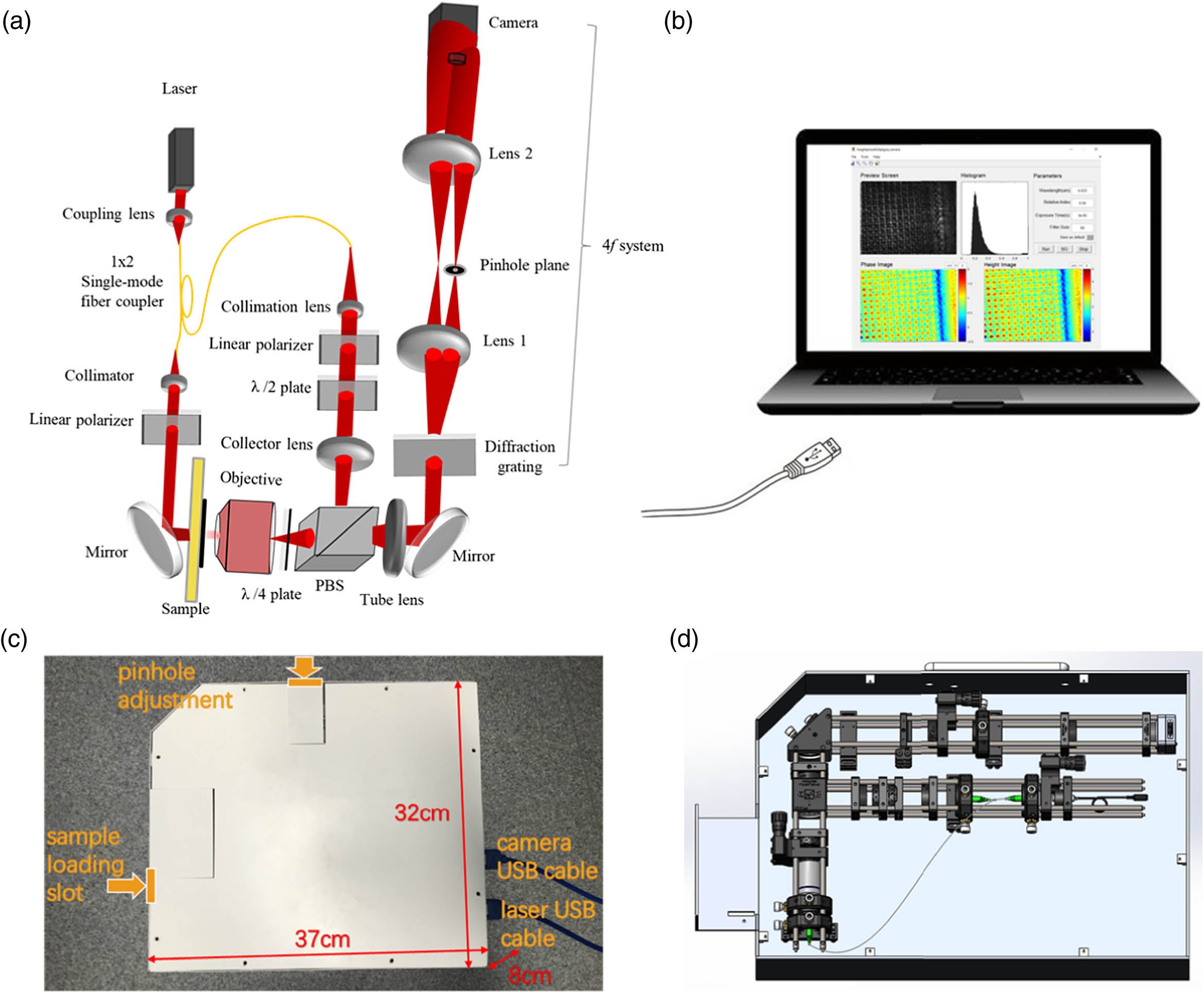
    Fig. 1. (a) Schematic design of the portable QPM system. (b) Software GUI running on the laptop. (c) Actual portable QPM system. (d) Internal components of the portable QPM system.
    (a) Histogram of the OPD values for all the pixels of all the frames. (b) Temporal fluctuation of the frame-averaged OPD value. (c) Histogram of the OPD standard deviation values. (d) OPD map averaged over all the frames.
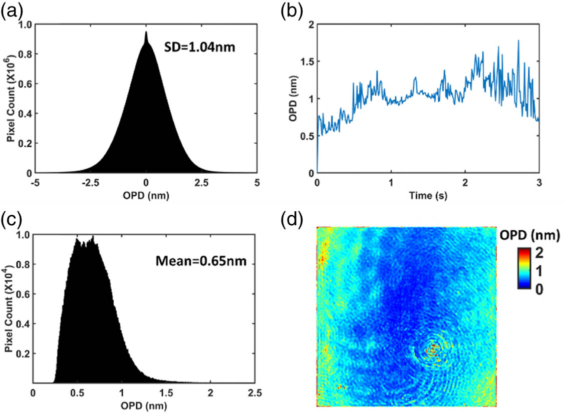
    Fig. 2. (a) Histogram of the OPD values for all the pixels of all the frames. (b) Temporal fluctuation of the frame-averaged OPD value. (c) Histogram of the OPD standard deviation values. (d) OPD map averaged over all the frames.
    (a) Typical SEM image for a portion of the NIST reference material (RM) 8820 sample showing the L500 nm S500 nm and L500 nm S1000 nm lines (figure adapted from Ref. [28]). (b) Phase map measured by the portable QPM system. Inset figure shows the line profile indicated by the white dotted line.
    Fig. 3. (a) Typical SEM image for a portion of the NIST reference material (RM) 8820 sample showing the L500 nm S500 nm and L500 nm S1000 nm lines (figure adapted from Ref. [28]). (b) Phase map measured by the portable QPM system. Inset figure shows the line profile indicated by the white dotted line.
    (a) Design of the gold electrodes in transistor sample. (b) Height map of the sample from the portable QPM system; inset figure shows the line profile along the white dotted line in (b). (c) AFM image of the sample (Software: NanoScope Analysis 1.5); inset figure shows the line profile along the white dotted line in (c). (d) Height histogram of the Au structure area and the bottom area selected in (b). (e) Height histogram of the Au structure area and the bottom area selected in (c).
    Fig. 4. (a) Design of the gold electrodes in transistor sample. (b) Height map of the sample from the portable QPM system; inset figure shows the line profile along the white dotted line in (b). (c) AFM image of the sample (Software: NanoScope Analysis 1.5); inset figure shows the line profile along the white dotted line in (c). (d) Height histogram of the Au structure area and the bottom area selected in (b). (e) Height histogram of the Au structure area and the bottom area selected in (c).
    (a) Height map of 5 μm beads. (b) Line profile along the yellow arrow direction for the bead indicated in (a).
    Fig. 5. (a) Height map of 5 μm beads. (b) Line profile along the yellow arrow direction for the bead indicated in (a).
    (a) Height map for a selected region in the NIST reference material (RM) 8820 sample. (b) Zoom-in height map for the selected area in (a). (c) SEM image of the selected area (figure adapted from Ref. [28]). (d) Histogram of the topography map in (b).
    Fig. 6. (a) Height map for a selected region in the NIST reference material (RM) 8820 sample. (b) Zoom-in height map for the selected area in (a). (c) SEM image of the selected area (figure adapted from Ref. [28]). (d) Histogram of the topography map in (b).
    (a) Raw interferogram of the RBCs with a zoom-in showing the fringe contrast and bending. (b) Retrieved height map of the RBCs in (a). (c) Snapshot of the membrane height fluctuation in Visualization 1 for the RBC selected in (b).
    Fig. 7. (a) Raw interferogram of the RBCs with a zoom-in showing the fringe contrast and bending. (b) Retrieved height map of the RBCs in (a). (c) Snapshot of the membrane height fluctuation in Visualization 1 for the RBC selected in (b).
    (a) Actual microfluidic device and the geometry of the channels. (b) Representative phase image showing the imaging field of view of the microfluidic channel. (c) Histogram of the dry mass for all the cells captured in the microfluidic channel. (d) Phase maps of a few selected myoblasts captured in the microfluidic channel.
    Fig. 8. (a) Actual microfluidic device and the geometry of the channels. (b) Representative phase image showing the imaging field of view of the microfluidic channel. (c) Histogram of the dry mass for all the cells captured in the microfluidic channel. (d) Phase maps of a few selected myoblasts captured in the microfluidic channel.
    Mengxuan Niu, Gang Luo, Xin Shu, Fuyang Qu, Shuang Zhou, Yi-Ping Ho, Ni Zhao, Renjie Zhou. Portable quantitative phase microscope for material metrology and biological imaging[J]. Photonics Research, 2020, 8(7): 1253
    Download Citation