Chandrasekar Perumal Veeramalai, Shuai Feng, Xiaoming Zhang, S. V. N. Pammi, Vincenzo Pecunia, Chuanbo Li, "Lead–halide perovskites for next-generation self-powered photodetectors: a comprehensive review," Photonics Res. 9, 968 (2021)

Search by keywords or author
- Photonics Research
- Vol. 9, Issue 6, 968 (2021)
![(a), (b) Schematic crystal structure of representative perovskite materials CH3NH3PbI3 and CsPbBr3, simulated from Vesta.3 Software; (c) comparative optical absorption behavior of semiconducting materials. Reproduced from Ref. [6] with permission. Copyright 2014, Springer Nature.](/richHtml/prj/2021/9/6/06000968/img_001.jpg)
Fig. 1. (a), (b) Schematic crystal structure of representative perovskite materials CH 3 NH 3 PbI 3 and CsPbBr 3 , simulated from Vesta.3 Software; (c) comparative optical absorption behavior of semiconducting materials. Reproduced from Ref. [6] with permission. Copyright 2014, Springer Nature.

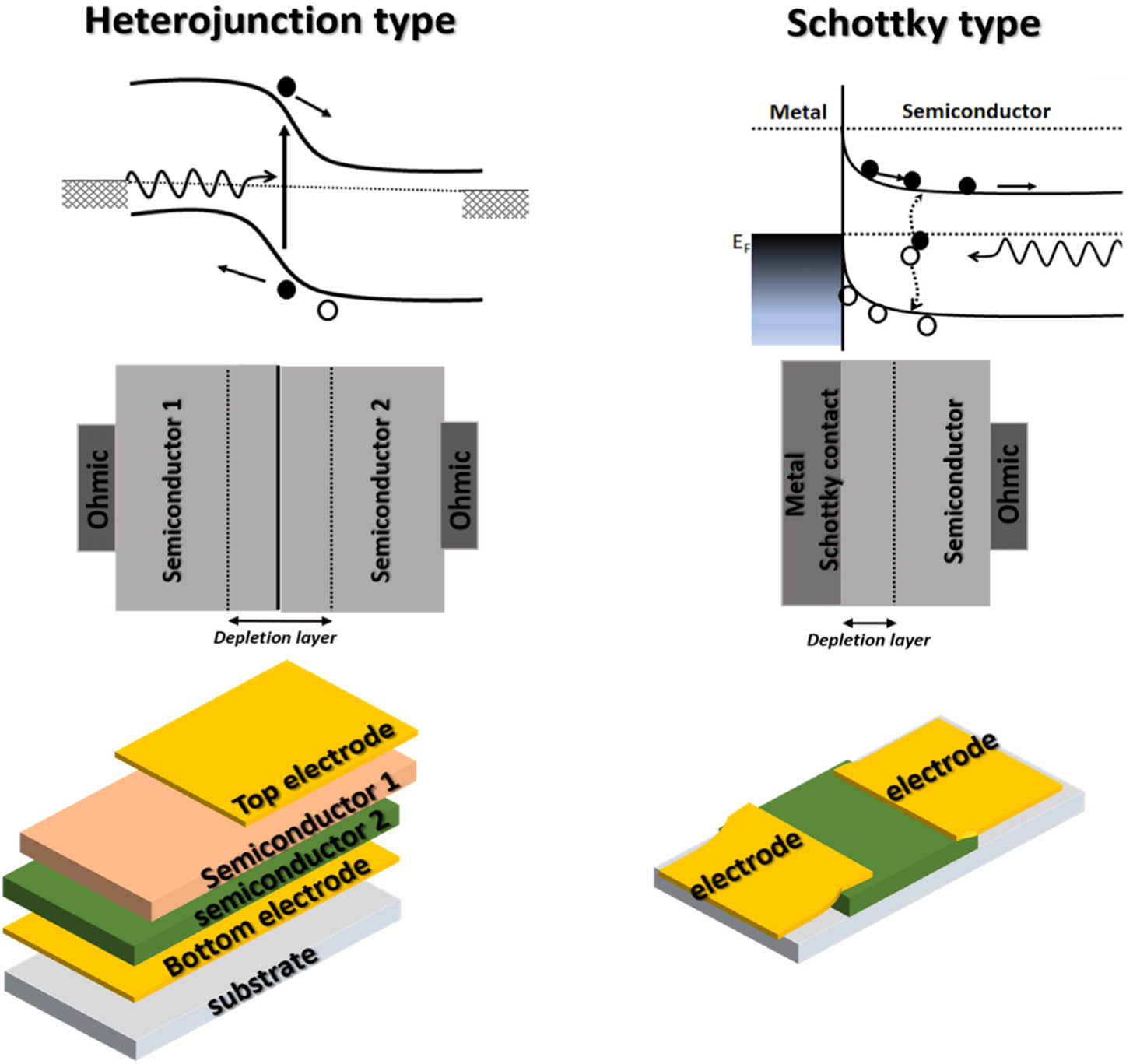
Fig. 2. Schematic diagrams of working principle of SPPDs in PV mode: heterojunction type (left side) and Schottky type (right side).
![(a) Preparation process of the MAPbBr3/MAPbIxBr3−x heterojunction; (b) responsivity of APbBr3/MAPbIxBr3−x and single crystal MAPbBr3 PDs at zero bias under the incident light with wavelengths of 350–800 nm and 400–800 nm, respectively; (c) schematic energy level diagram at the MAPbBr3/MAPbIxBr3−x junction under irradiation. Reproduced with permission from Ref. [56]. Copyright 2016, American Institute of Physics. (d) Photographic image of the as-grown heterostructure single crystal (top); SEM image of the heterostructure interface (bottom). (e) Band diagram of the (4-AMP)(MA)2Pb3Br10/MAPbBr3 heterostructure detector; (f) plots of the R and D* as a function of light intensity; (g) response speed of (4-AMP)(MA)2Pb3Br10/MAPbBr3 heterostructure device at rise edges and fall edges. Reproduced with permission from Ref. [57]. Copyright 2020, Wiley-VCH. (h) Schematic illustration of the Au–Al electrodes separated by 30 μm on MAPbI3 single crystal; (i) schematic illustration of the working mechanism for Schottky junction based on asymmetric electrodes; (j) photocurrent response of Au/MAPbI3/Al device at different wavelengths; (k) spectral photoresponsivity of MAPbI3 single crystal PD. Reproduced with permission from Ref. [58]. Copyright 2016, Royal Society of Chemistry.](/Images/icon/loading.gif)
Fig. 3. (a) Preparation process of the MAPbBr 3 / MAPbI x Br 3 − x heterojunction; (b) responsivity of APbBr 3 / MAPbI x Br 3 − x and single crystal MAPbBr 3 PDs at zero bias under the incident light with wavelengths of 350–800 nm and 400–800 nm, respectively; (c) schematic energy level diagram at the MAPbBr 3 / MAPbIxBr 3 − x junction under irradiation. Reproduced with permission from Ref. [56]. Copyright 2016, American Institute of Physics. (d) Photographic image of the as-grown heterostructure single crystal (top); SEM image of the heterostructure interface (bottom). (e) Band diagram of the ( 4 -AMP ) ( MA ) 2 Pb 3 Br 10 / MAPbBr 3 heterostructure detector; (f) plots of the R and D * as a function of light intensity; (g) response speed of ( 4 -AMP ) ( MA ) 2 Pb 3 Br 10 / MAPbBr 3 heterostructure device at rise edges and fall edges. Reproduced with permission from Ref. [57]. Copyright 2020, Wiley-VCH. (h) Schematic illustration of the Au–Al electrodes separated by 30 μm on MAPbI 3 single crystal; (i) schematic illustration of the working mechanism for Schottky junction based on asymmetric electrodes; (j) photocurrent response of Au / MAPbI 3 / Al device at different wavelengths; (k) spectral photoresponsivity of MAPbI 3 single crystal PD. Reproduced with permission from Ref. [58]. Copyright 2016, Royal Society of Chemistry.
![(a) Photographic image of CsPbBr3 single crystal; (b) I-V curve of device Au/CsPbBr3/Pt in dark and under illumination; (c) photoresponse of device Au/CsPbBr3/Pt under light pulses measured under zero bias. Reproduced with permission from Ref. [28]. Copyright 2017, Wiley-VCH. (d) Carrier separation transmission diagram of the device based on CH3NH3PbI3 single crystal PD; (e) variation of light responsivity of devices with different channel widths; (f) dependence of responsivity and on–off ratio on the light intensity. Reproduced with permission from Ref. [60]. Copyright 2021, Elsevier.](/Images/icon/loading.gif)
Fig. 4. (a) Photographic image of CsPbBr 3 single crystal; (b) I -V curve of device Au / CsPbBr 3 / Pt in dark and under illumination; (c) photoresponse of device Au / CsPbBr 3 / Pt under light pulses measured under zero bias. Reproduced with permission from Ref. [28]. Copyright 2017, Wiley-VCH. (d) Carrier separation transmission diagram of the device based on CH 3 NH 3 PbI 3 single crystal PD; (e) variation of light responsivity of devices with different channel widths; (f) dependence of responsivity and on–off ratio on the light intensity. Reproduced with permission from Ref. [60]. Copyright 2021, Elsevier.
![(a) Schematic illustration of MAPbI3 NC synthesis; (b) TEM image of MAPbI3 NCs (the inset shows MAPbI3 nanocrystal size distribution plot); (c) schematic diagram of the MAPbI3 NC based self-powered PD; (d) J-V curves of the MAPbI3 NC-based self-powered PD under 808 nm illumination; (e) photocurrent versus time for the PD under light on/off cycles at 0 V under 808 nm illumination. Reproduced with permission from Ref. [50]. Copyright 2020, Wiley-VCH. (f) Cross-sectional SEM image of ITO/ZnO(70 nm)/CdS(150 nm) /CsPbBr3(200 nm)/Au trilayer PDs; (g) I-V curve of trilayer PD device in dark and under 85 μW cm−2 405 nm illumination; (h) potential charges generation and transportation process under 85 μW cm−2 405 nm illumination illustrated by band diagram. Reproduced with permission from Ref. [67]. Copyright 2020, Institute of Physics.](/Images/icon/loading.gif)
Fig. 5. (a) Schematic illustration of MAPbI 3 NC synthesis; (b) TEM image of MAPbI 3 NCs (the inset shows MAPbI 3 nanocrystal size distribution plot); (c) schematic diagram of the MAPbI 3 NC based self-powered PD; (d) J -V curves of the MAPbI 3 NC-based self-powered PD under 808 nm illumination; (e) photocurrent versus time for the PD under light on/off cycles at 0 V under 808 nm illumination. Reproduced with permission from Ref. [50]. Copyright 2020, Wiley-VCH. (f) Cross-sectional SEM image of ITO/ZnO(70 nm)/CdS(150 nm) /CsPbBr 3 ( 200 nm ) / Au trilayer PDs; (g) I -V curve of trilayer PD device in dark and under 85 μW cm − 2 405 nm illumination; (h) potential charges generation and transportation process under 85 μW cm − 2 405 nm illumination illustrated by band diagram. Reproduced with permission from Ref. [67]. Copyright 2020, Institute of Physics.
![(a) Schematic illustration of the synthesis process of the CsPbBr3 NWs and CsPbBr3 micro- and nanostructures; (b) schematic illustration of the perovskite NW PD; (c) energy band diagram of the perovskite NW PD. (d) J-t curve at the light intensity of 6.4×10⁻⁴ mW cm−2; (e) responsivity and detectivity of the device under various optical power. Reproduced with permission from Ref. [68]. Copyright 2018, Elsevier. (f) Schematic illustration of the fabrication process of the P3PCS PD; (g) CsPbBr3 nanowire array; (h) schematic of device structure; (i) responsivity and detectivity curves of P3PCS device; (j) long-term photoresponse curves of P3PCS device under 100 mW cm−2 white light at 0 V. Reproduced with permission from Ref. [69]. Copyright 2019, Wiley-VCH.](/Images/icon/loading.gif)
Fig. 6. (a) Schematic illustration of the synthesis process of the CsPbBr 3 NWs and CsPbBr 3 micro- and nanostructures; (b) schematic illustration of the perovskite NW PD; (c) energy band diagram of the perovskite NW PD. (d) J -t curve at the light intensity of 6.4 × 10 − 4 mW cm − 2 ; (e) responsivity and detectivity of the device under various optical power. Reproduced with permission from Ref. [68]. Copyright 2018, Elsevier. (f) Schematic illustration of the fabrication process of the P3PCS PD; (g) CsPbBr 3 nanowire array; (h) schematic of device structure; (i) responsivity and detectivity curves of P3PCS device; (j) long-term photoresponse curves of P3PCS device under 100 mW cm − 2 white light at 0 V. Reproduced with permission from Ref. [69]. Copyright 2019, Wiley-VCH.
![(a) SEM image of CsPbBr3 microplatelets shows sharp edge and smooth surface morphology. (b) Schematic layout of the perovskite CsPbBr3 microplatelets PD based on vertical Schottky junction structure; (c) I-V characteristics of the CsPbBr3 microplatelets PD under 405 nm light illumination with different density; (d) normalized I-t curves of CsPbBr3 microplatelets PD with long-term storage without encapsulation. Reproduced with permission from Ref. [75]. Copyright 2020, Royal Society of Chemistry. (e) Schematic of fabricating process of the CsPbBr3 microcrystal-based PD; (f) room temperature spectral responsivity curves of the CsPbBr3 microcrystal-based PD at 0 V bias. Reproduced with permission from Ref. [76]. Copyright 2019, American Chemical Society. (g) SEM image of CsPbBr3 microcrystal perovskite film. The inset is a digital photograph of the perovskite film under 365 nm purple flashlight. (h) Schematic illustration of the CsPbBr3 microcrystal perovskite PD; (i) power-dependent R and D*CsPbBr3 microcrystal perovskite PD under 0 V bias. Reproduced with permission from Ref. [77]. Copyright 2019, American Chemical Society.](/Images/icon/loading.gif)
Fig. 7. (a) SEM image of CsPbBr 3 microplatelets shows sharp edge and smooth surface morphology. (b) Schematic layout of the perovskite CsPbBr 3 microplatelets PD based on vertical Schottky junction structure; (c) I -V characteristics of the CsPbBr 3 microplatelets PD under 405 nm light illumination with different density; (d) normalized I -t curves of CsPbBr 3 microplatelets PD with long-term storage without encapsulation. Reproduced with permission from Ref. [75]. Copyright 2020, Royal Society of Chemistry. (e) Schematic of fabricating process of the CsPbBr 3 microcrystal-based PD; (f) room temperature spectral responsivity curves of the CsPbBr 3 microcrystal-based PD at 0 V bias. Reproduced with permission from Ref. [76]. Copyright 2019, American Chemical Society. (g) SEM image of CsPbBr 3 microcrystal perovskite film. The inset is a digital photograph of the perovskite film under 365 nm purple flashlight. (h) Schematic illustration of the CsPbBr 3 microcrystal perovskite PD; (i) power-dependent R and D * CsPbBr 3 microcrystal perovskite PD under 0 V bias. Reproduced with permission from Ref. [77]. Copyright 2019, American Chemical Society.
![(a) Device structure of the hybrid perovskite PD; (b) LDR of the PD with the device structure ITO/PEDOT:PSS/CH3NH3PbI3−xClx/PCBM/PFN/Al. The PD has a large LDR of 4100 dB. Reproduced with permission from Ref. [85]. Copyright 2014, Springer Nature. (c) SEM image of MAPbI3−xClx thin films on glass substrate; (d) schematic representation of a photodetector device configuration; (e) transient photocurrent properties of device under illumination at 632 nm; (f) long-term photo stability illuminated under 1000 μW/cm2 with different intervals up to 500 h. Reproduced with permission from Ref. [86]. Copyright 2020, Elsevier. (g) SEM image of PMMA-modified CsPbBr3 film; (h) schematic and cross-sectional SEM image of the as-fabricated PD with a structure of ITO/CsPbBr3/PMMA/Ag. Reproduced with permission from Ref. [87]. Copyright 2020, Royal Society of Chemistry. (i) Schematic structure of PD based on all-inorganic perovskite CsPbIxBr3−x; (j) current density-voltage (J-V) curves of CsPbIBr2-based PDs under dark and illumination of 450 nm monochrome light with intensity of 1 μm cm−2 to 1 mW cm−2; (k) photoresponsivity evolution of PDs based on inorganic perovskite CsPbIxBr3−x and hybrid perovskite MAPbI3 in air ambient condition without encapsulation. Reproduced with permission from Ref. [88]. Copyright 2018, Wiley-VCH. (l) Schematic illustration of as-fabricated self-powered PD based on CsxDMA1−xPbI3 perovskite films; (m) responsivity spectrum of the self-powered PD based on the film with CsI/DMAPbI3 molar ratio of 1:2 in the precursor at 0 V; (n) variation of spectral responsivity with time of the self-powered PD in air (10%–20% RH) at a bias voltage of 0 V under 532 nm illumination. Reproduced with permission from Ref. [89]. Copyright 2020, Elsevier. (o) Disordered state of ions under dark (upper) and mobile ions accumulated at the opposite interfaces under illumination due to the light-induced self-poling effect (lower), resulting in the built-in electric field; (p) energy band schematics of the MOS structure under dark before contact. Reproduced with permission from Ref. [90]. Copyright 2019, Royal Society of Chemistry.](/Images/icon/loading.gif)
Fig. 8. (a) Device structure of the hybrid perovskite PD; (b) LDR of the PD with the device structure ITO / PEDOT : PSS / CH 3 NH 3 PbI 3 − x Cl x / PCBM / PFN / Al . The PD has a large LDR of 4100 dB. Reproduced with permission from Ref. [85]. Copyright 2014, Springer Nature. (c) SEM image of MAPbI 3 − x Cl x thin films on glass substrate; (d) schematic representation of a photodetector device configuration; (e) transient photocurrent properties of device under illumination at 632 nm; (f) long-term photo stability illuminated under 1000 μW / cm 2 with different intervals up to 500 h. Reproduced with permission from Ref. [86]. Copyright 2020, Elsevier. (g) SEM image of PMMA-modified CsPbBr 3 film; (h) schematic and cross-sectional SEM image of the as-fabricated PD with a structure of ITO / CsPbBr 3 / PMMA / Ag . Reproduced with permission from Ref. [87]. Copyright 2020, Royal Society of Chemistry. (i) Schematic structure of PD based on all-inorganic perovskite CsPbI x Br 3 − x ; (j) current density-voltage (J -V ) curves of CsPbIBr 2 -based PDs under dark and illumination of 450 nm monochrome light with intensity of 1 μm cm − 2 to 1 mW cm − 2 ; (k) photoresponsivity evolution of PDs based on inorganic perovskite CsPbI x Br 3 − x and hybrid perovskite MAPbI 3 in air ambient condition without encapsulation. Reproduced with permission from Ref. [88]. Copyright 2018, Wiley-VCH. (l) Schematic illustration of as-fabricated self-powered PD based on Cs x DMA 1 − x PbI 3 perovskite films; (m) responsivity spectrum of the self-powered PD based on the film with CsI / DMAPbI 3 molar ratio of 1 : 2 in the precursor at 0 V; (n) variation of spectral responsivity with time of the self-powered PD in air (10%–20% RH) at a bias voltage of 0 V under 532 nm illumination. Reproduced with permission from Ref. [89]. Copyright 2020, Elsevier. (o) Disordered state of ions under dark (upper) and mobile ions accumulated at the opposite interfaces under illumination due to the light-induced self-poling effect (lower), resulting in the built-in electric field; (p) energy band schematics of the MOS structure under dark before contact. Reproduced with permission from Ref. [90]. Copyright 2019, Royal Society of Chemistry.
![(a) Device structure of self-powered PD with MAPbI3 as the photosensitive and triboelectric layer; (b) change of Voc upon repeated illumination that varies in intensity at 100 mW cm−2. Reproduced with permission from Ref. [93]. Copyright 2015, American Chemical Society. (c) Schematic of a triboelectric-assisted perovskite PD showing charge carrier separation assisted by the triboelectric charges created by the TENG; (d) schematic diagram and the working principle of the (+) triboelectric-assisted perovskite PD; (e) transient photoresponse of the triboelectric-actuated perovskite PD (blue) and perovskite PD without assistance of triboelectricity (red) under alternating on–off laser light (50 mW) illumination with a 3 Hz chopping frequency. Reproduced with permission from Ref. [94]. Copyright 2019, Elsevier.](/Images/icon/loading.gif)
Fig. 9. (a) Device structure of self-powered PD with MAPbI 3 as the photosensitive and triboelectric layer; (b) change of V oc upon repeated illumination that varies in intensity at 100 mW cm − 2 . Reproduced with permission from Ref. [93]. Copyright 2015, American Chemical Society. (c) Schematic of a triboelectric-assisted perovskite PD showing charge carrier separation assisted by the triboelectric charges created by the TENG; (d) schematic diagram and the working principle of the (+) triboelectric-assisted perovskite PD; (e) transient photoresponse of the triboelectric-actuated perovskite PD (blue) and perovskite PD without assistance of triboelectricity (red) under alternating on–off laser light (50 mW) illumination with a 3 Hz chopping frequency. Reproduced with permission from Ref. [94]. Copyright 2019, Elsevier.
![(a) Plane-view SEM image of CsPbBr3 perovskite thin films Al2O3-modified FTO substrates; (b) photoresponse curves of CsPbBr3 perovskite PDs, Al2O3/CsPbBr3 perovskite PDs, and Al2O3/CsPbBr3/TiO2 perovskite PDs, respectively; (c) energy band diagram of heterojunctions; (d) current–voltage (I-V) curves of PDs under dark and illumination of 405 nm laser with intensity of 6.2 μW cm−2 to 114 mW cm−2; (e) photoresponse curves of ACT PDs under modulated 405 nm laser with various light intensity (0 V); (f) light current and dark current stability at different days for hard substrate device; (g) light current and dark current of flexible device after different bending cycles. Reproduced with permission from Ref. [123]. Copyright 2019, Wiley-VCH.](/Images/icon/loading.gif)
Fig. 10. (a) Plane-view SEM image of CsPbBr 3 perovskite thin films Al 2 O 3 -modified FTO substrates; (b) photoresponse curves of CsPbBr 3 perovskite PDs, Al 2 O 3 / CsPbBr 3 perovskite PDs, and Al 2 O 3 / CsPbBr 3 / TiO 2 perovskite PDs, respectively; (c) energy band diagram of heterojunctions; (d) current–voltage (I -V ) curves of PDs under dark and illumination of 405 nm laser with intensity of 6.2 μW cm − 2 to 114 mW cm − 2 ; (e) photoresponse curves of ACT PDs under modulated 405 nm laser with various light intensity (0 V); (f) light current and dark current stability at different days for hard substrate device; (g) light current and dark current of flexible device after different bending cycles. Reproduced with permission from Ref. [123]. Copyright 2019, Wiley-VCH.
![(a) FESEM image of a typical PD with Au/Ag electrode pair; (b) I-V curves of the CH3NH3PbI3 MWs array-based PDs with asymmetric contact electrodes (Au/Ag, Au/Al); (c) histogram of Voc and Isc for devices with different asymmetric electrode pairs; (d) dark current and photocurrent of the flexible PD being bent to various radii. Reproduced with permission from Ref. [71]. Copyright 2019, Wiley-VCH. (e) Device structure and (f) cross-sectional SEM image of MAPbI3:graphene QD based PD. (g) NEP/spectral detectivity of PD. The inset shows excellent flexibility of the PD. (h) Evolution of responsivity during repeated 1000 bending cycles at λ=600 nm and d=4 mm. Reproduced with permission from Ref. [124]. Copyright 2019, American Chemical Society.](/Images/icon/loading.gif)
Fig. 11. (a) FESEM image of a typical PD with Au/Ag electrode pair; (b) I -V curves of the CH3NH3PbI3 MWs array-based PDs with asymmetric contact electrodes (Au/Ag, Au/Al); (c) histogram of V o c and I s c for devices with different asymmetric electrode pairs; (d) dark current and photocurrent of the flexible PD being bent to various radii. Reproduced with permission from Ref. [71]. Copyright 2019, Wiley-VCH. (e) Device structure and (f) cross-sectional SEM image of MAPbI 3 : graphene QD based PD. (g) NEP/spectral detectivity of PD. The inset shows excellent flexibility of the PD. (h) Evolution of responsivity during repeated 1000 bending cycles at λ = 600 nm and d = 4 mm . Reproduced with permission from Ref. [124]. Copyright 2019, American Chemical Society.
![(a) Schematic illustration of ferroelectric polarization-induced formation of internal electric field in the nanowire array device; (b) schematic illustration of the fabrication process of flexible P(VDF-TrFE)/perovskite hybrid nanowire arrays-based PD; (c) 650 nm wavelength light illumination of flexible P(VDF-TrFE)/perovskite PDs with various power intensities at 0 V; (d) I-t curves of the poled perovskite-0.6 device under 650 nm light illumination at bending angles with the intersection angle between bending direction and nanowire direction of 0°. Reproduced with permission from Ref. [125]. Copyright 2019, Wiley-VCH. (e) I-t curve of flexible P(VDF-TrFE)/perovskite PDs at different bending cycles. Reproduced with permission from Ref. [126]. Copyright 2019, Wiley-VCH.](/Images/icon/loading.gif)
Fig. 12. (a) Schematic illustration of ferroelectric polarization-induced formation of internal electric field in the nanowire array device; (b) schematic illustration of the fabrication process of flexible P(VDF-TrFE)/perovskite hybrid nanowire arrays-based PD; (c) 650 nm wavelength light illumination of flexible P(VDF-TrFE)/perovskite PDs with various power intensities at 0 V; (d) I -t curves of the poled perovskite-0.6 device under 650 nm light illumination at bending angles with the intersection angle between bending direction and nanowire direction of 0°. Reproduced with permission from Ref. [125]. Copyright 2019, Wiley-VCH. (e) I -t curve of flexible P(VDF-TrFE)/perovskite PDs at different bending cycles. Reproduced with permission from Ref. [126]. Copyright 2019, Wiley-VCH.
![(a) Schematic diagram of the SFPDs with integrated TENG; (b) change in the measured voltage (ΔV) and voltage responsivity of the device at different light intensities; (c) ΔV at various angles of incident light. Reproduced with permission from Ref. [129]. Copyright 2018, Wiley-VCH. (d) Schematic illustration of the integrated nanosystem, consisting of an energy conversion unit, a light sensing unit, and a current measurement system. (e) J-V curves of the as-fabricated integrated perovskite solar cell; (f) photoresponse curves after 100 and 200 bending cycles. Reproduced with permission from Ref. [130]. Copyright 2016, Wiley-VCH.](/Images/icon/loading.gif)
Fig. 13. (a) Schematic diagram of the SFPDs with integrated TENG; (b) change in the measured voltage (Δ V ) and voltage responsivity of the device at different light intensities; (c) Δ V at various angles of incident light. Reproduced with permission from Ref. [129]. Copyright 2018, Wiley-VCH. (d) Schematic illustration of the integrated nanosystem, consisting of an energy conversion unit, a light sensing unit, and a current measurement system. (e) J -V curves of the as-fabricated integrated perovskite solar cell; (f) photoresponse curves after 100 and 200 bending cycles. Reproduced with permission from Ref. [130]. Copyright 2016, Wiley-VCH.
![(a) Photoresponsivity evolution of PDs based on inorganic perovskite CsPbIxBr3−x and hybrid perovskite MAPbI3 at 100°C in N2 ambient condition. XRD spectra and digital photographs of (b) CsPbIBr2 and (c) MAPbI3 devices before and after heated at 100°C in N2-filled glove box for 244 h. The obvious PbI2 peak in XRD spectrum of MAPbI3 devices after being heated indicates the decomposition of MAPbI3. Reproduced with permission from Ref. [88]. Copyright 2018, Wiley-VCH. (d) Thermal stability of MAPbI3 NCs; photographic image of samples under 365 nm illumination. The samples are annealed at 40°C, 50°C, 60°C, 70°C, and 80°C for 10 min in open air. Reproduced with permission from Ref. [50]. Copyright 2020, Wiley-VCH.](/Images/icon/loading.gif)
Fig. 14. (a) Photoresponsivity evolution of PDs based on inorganic perovskite CsPbI x Br 3 − x and hybrid perovskite MAPbI 3 at 100°C in N 2 ambient condition. XRD spectra and digital photographs of (b) CsPbIBr 2 and (c) MAPbI 3 devices before and after heated at 100°C in N 2 -filled glove box for 244 h. The obvious PbI 2 peak in XRD spectrum of MAPbI 3 devices after being heated indicates the decomposition of MAPbI 3 . Reproduced with permission from Ref. [88]. Copyright 2018, Wiley-VCH. (d) Thermal stability of MAPbI 3 NCs; photographic image of samples under 365 nm illumination. The samples are annealed at 40°C, 50°C, 60°C, 70°C, and 80°C for 10 min in open air. Reproduced with permission from Ref. [50]. Copyright 2020, Wiley-VCH.
|
Table 1. Basic Characteristic Physical Parameters of Perovskite Materials
|
Table 2. Summary of Key Parameters of Perovskite-Based SPPDs
|
Table 3. Summary of Flexible Self-Powered Perovskite-Based PDs

Set citation alerts for the article
Please enter your email address