
Yifan Li, Yating Zhang, Yu Yu, Zhiliang Chen, Qingyan Li, Tengteng Li, Jie Li, Hongliang Zhao, Quan Sheng, Feng Yan, Zhen Ge, Yuxin Ren, Yongsheng Chen, Jianquan Yao. Ultraviolet-to-microwave room-temperature photodetectors based on three-dimensional graphene foams[J]. Photonics Research, 2020, 8(3): 368
- Photonics Research
- Vol. 8, Issue 3, 368 (2020)
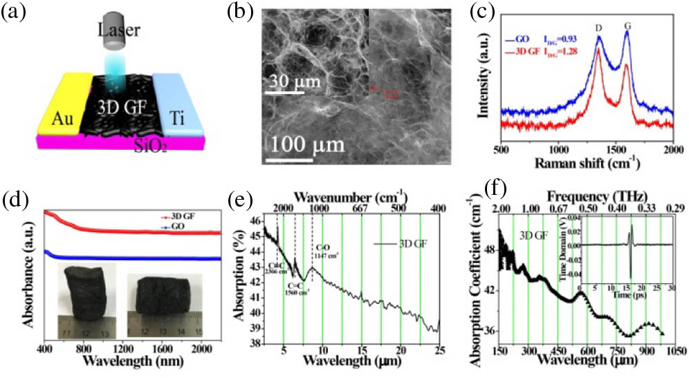
Fig. 1. (a) Schematic structure of the 3D GF photodetector. (b) SEM image of the 3D GF with the magnification scales of 100 μm and 10 μm. (c) Raman spectra of 3D GF (red line) and GO (blue line). (d) Absorption spectra of 3D GF (red line) and GO (blue line) over the range from 400 to 2200 nm. The inset pictures exhibit the 3D GF columnar. (e) FTIR spectrum of 3D GF ranging from 2.5 to 25 μm. (f) The THz-TDS spectrum of 3D GF ranging from 150 to 1000 μm.
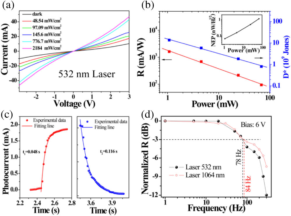
Fig. 2. (a) Current–voltage (I–V ) characteristics in the dark and with different illumination intensities of the 532 nm laser. (b) The logarithmic photoresponsivity (left) and detectivity (right) as a function of logarithmic optical power at 0.1 V bias voltage. Inset is noise-equivalent power (NEP) as a function of logarithmic optical power at the same condition. (c) Time response characteristic curves of the device at 0.5 V bias voltage. (d) Frequency response characteristic under 532 nm and 1064 nm lasers.
Fig. 3. Double-logarithmic coordinates’ photoresponsivities to laser power under (a) 10.6 μm, (b) 118 μm, and (c) 1.36 mm lasers at 0.1 V voltage. Corresponding insets are the switched photocurrent under different irradiances. (d) The broadband photoresponsivity over a wavelength range of 300–2200 nm under different bias voltages (0.06, 1, 5 V). Inset is the applified R R β
Fig. 4. (a) Photocurrent generation schematic of the 3D GF PD under 532 mm laser illumination. The illumination is localized in the middle of the channel. The x T ( x ) S ( x ) Δ V ( x ) = Δ S Δ T ( x ) I–V characteristics of Au/3D GF/Ti and Au/3D GF/Au structures. (d) I–V characteristics of Au/3D GF/Ti under different 532 nm laser illumination intensities. (e) The photocurrent responses of the two different Au/3D GF/Ti and Au/3D GF/Au devices under 532 nm illumination with irradiance of 50 mW · cm − 2
Fig. 5. (a) Temperature distributions of the device at dark and at laser illumination (532 nm, 1 mW). Inset: the MIR image of the device under dark and laser illumination. (b) The temperature (top) and photocurrent (bottom) curves as a function of time at 0.05 V positive bias voltage. (c) I–V characteristics at 532 nm laser of 50 mW / cm 2 50 mW / cm 2

Set citation alerts for the article
Please enter your email address
© Copyright 2018-2021 | Chinese Laser Press. All Rights Reserved 沪ICP备15018463号-20