1School of Information Science and Engineering (ISE), Shandong University, Qingdao 266000, China
2Shandong Sinochip Semiconductors Co. Ltd, Jinan 250101, China
3Neumem Co., Ltd, Hefei 230088, China
4Key Laboratory of Microelectronic Devices and Integrated Technology, Institute of Microelectronics of Chinese Academy of Sciences, Beijing 100029, China
The “memory wall” of traditional von Neumann computing systems severely restricts the efficiency of data-intensive task execution, while in-memory computing (IMC) architecture is a promising approach to breaking the bottleneck. Although variations and instability in ultra-scaled memory cells seriously degrade the calculation accuracy in IMC architectures, stochastic computing (SC) can compensate for these shortcomings due to its low sensitivity to cell disturbances. Furthermore, massive parallel computing can be processed to improve the speed and efficiency of the system. In this paper, by designing logic functions in NOR flash arrays, SC in IMC for the image edge detection is realized, demonstrating ultra-low computational complexity and power consumption (25.5 fJ/pixel at 2-bit sequence length). More impressively, the noise immunity is 6 times higher than that of the traditional binary method, showing good tolerances to cell variation and reliability degradation when implementing massive parallel computation in the array.
1. Introduction
In traditional von Neumann architecture, data is frequently transferred between the processing unit and the memory unit, which causes significant power consumption and seriously limits processing efficiency. In-memory computing (IMC), wherein memory units designed with the capability to store data and execute computational tasks simultaneously, has been proposed as a promising approach to solve this issue and break the “memory wall”. Recently, many impressive IMCs have been reported by using commercial memories (SRAM, DRAM, flash) and emerging memories (ReRAM, PRAM, etc.)[1-3]. For data-intensive computing tasks, it is necessary to construct a large memory array for large-matrix computation, which means that the current of each memory cell has to be low so that the accumulated currents will not exceed the capability of the sensing amplifier (SA)[3]. At the same time, the leakage currents in the array should be suppressed to reduce power consumption. As a non-volatile memory, flash memory has matured the fabrication process with good reliabilities, abilities to construct large memory arrays, and good compatibility with peri-circuits. All these make flash memory a promising candidate to meet the stringent requirements of data-intensive tasks.
Stochastic computing (SC) is one type of approximate calculation, which is an effective approach for data-intensive tasks. SC is implemented based on probabilistic calculations with inherent tolerance for noise, as shown inFig. 1(a). Besides, SC shows great potential to simplify the hardware circuits and allows massively parallel computations towards realizing complex calculations in simple logic circuits[4]. It is anticipated that SC could be utilized in applications requiring high-speed processing for single-target detection.
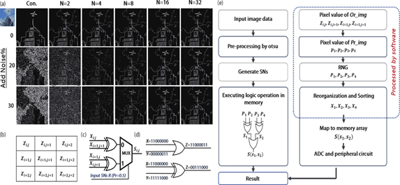
Figure 1.(Color online) (a) Comparison between conventional and SC methods, SNs length =N bits. (b) Region of the image. (c) The stochastic computational element to realize image detection algorithmic in logic circuits. (d) Scaled addition realized by the OR gate, scaled subtraction, and absolute value calculation realized by the XOR gate. (e) The data processing flow chart in the proposed method.
So far, most works are more focused on computing complexity or merely accuracy[5], while the studies on the tradeoff of these two contradictory aspects are still limited[6]. In this work, a novel IMC architecture is designed to perform SC process for image edge detection, which provides an effective solution to address the concerns of power consumption and accuracy simultaneously.
In this work, a flash-based high-efficiency and high-precision SC strategy has been proposed, which can effectively reduce computational complexity and power consumption while retaining accuracy and interference immunity. Massive parallel operations in a large memory array have also been achieved by a novel and simple IMC architecture.
2. Implementing IMC by flash memory
The flow chart of the method is shown inFig. 1(e). After the pre-processing of an image, the generated stochastic numbers (SNs) input to the memory array, can be applied in the image edge detection.
2.1. Pre-processing
SC with longer SNs improves computing accuracy, but power consumption and delay will increase. To address this concern, the image can be pre-processed by the Otsu algorithm before computing[7]. Here we adopted the extended 2D Otsu to segment the pixel value of the image into three levels. The pixel values of these three levels are set to 0, 0.5, and 1. That is, each pixel value of this image is represented by the SNs with the probability value of 0, 0.5, and 1. By this means, only SNs with 50% probability needed to be computed. The overhead of a random number generator (RNG) is greatly reduced, thus decreasing the computational complexity. Besides, SNs with a 50% probability are easier to be generated by the true random number generator (TRNG), eliminating the computational trouble caused by correlation terms among SNs. Although power consumption and computational complexity are reduced, the simulation results show that it can still maintain high computational accuracy. Therefore, the required SNs are generated according to the values after three-valued segmentation processing.
2.2. Logic operations in NOR flash
After image processing and SN generating, the logic in memory operation can be implemented by NOR flash memory. Logic operations in IMC are based on Ohm's law and the Kirchhoff's law, which utilizes the cel0-ls’ characteristics and the designed array to perform calculations.Fig. 2(a) shows the basic structure of the flash cells, andFig. 2(b) shows the basic current curves. In this work, we choose the sub-saturation region as the operation region, and the source-line current (ISL) can be expressed by Eq. (1),
Figure 2.(Color online) (a) The NOR flash architecture for logic operation. (b)I–V curve for NOR flash array. (c) Memory window degradation by P/E cycling. (d) Read current fluctuations can be observed caused by RTN.
wherew is a constant referring to the feature of devices;VD,VG, andVth represent the drain bias, the gate bias, and the cell threshold voltages, respectively.Vth in each memory cell can be tuned by using erasing and programming. The entire computational process is implemented in a large array, and the number of rows enabled in the array is related to the length of the input sequence. In this way, logic operations can be implemented in the flash memory array. For example, AND operation can be accomplished by mapping in1 toVG1, and mapping in2 toVth1, thusISL can represent the logic results. Only whenVG1 andVth1 are both 1, the result is 1. Other logic operations also can be realized by combing device properties and the design of flash arrays.
Along with the memory scaling, the variations of cells will have a much larger impact on the accuracy of calculations[8]. Firstly, the work regions should be optimized because largeVD (the saturation region) will result in high power consumption while lowVD (the linear region) will suffer from serious variation effects. Secondly, the repeated cycling will inevitably cause memory window degradation due toVth shifts, as shown inFig. 2(c). In addition, the read noise will be serious, such as the enhanced random telegraph noise (RTN) that is caused by the traps in the tunneling oxide. For one single trap, there are two current levels at the fixed read conditions, and the current fluctuation is shown inFig. 2(d). Scaling the cell size will further increase the fluctuations, leading to larger read current instability. All these should be well investigated for identifying the noise tolerance boundary of the designed memory array. In this work, we take the sub-saturation region (VD = 1 V) to implement the calculations in IMC to suppress the impacts ofVD variations and guarantee low power consumption.
2.3. Image edge detection by SC
The Roberts cross kernel[9] is one of the most common edge detection operators that can be converted into simple logic operations in SC. It is easy to be adopted in IMC to implement low-precision and data-intensive applications. The Roberts cross kernel consists of two 2 × 2 conventional kernels. The magnitude result is described as Eq. (2) when considering the 3 × 3 region inFig. 1(b).
whereS(i,j) andZi,j represent the results of edge detection and the pixel value of the original image at (i,j), respectively. According to Eq. (2), we need to convert the scaled addition, the scaled subtraction, and the absolute value calculation into logic circuits respectively[4]. The scaled addition is implemented by the multiplexer. In addition, it also can be done by the OR gate. The scaled subtraction and absolute value calculation can be implemented by the XOR gate, as shown inFigs. 1(c) and1(d).
As the key of the proposed method, the SNs are mapped into the NOR flash memory array to implement the Roberts cross kernel in Eq. (1). After XOR operations in |Zi,j –Zi+1,j+1 | and |Zi+1,j –Zi,j+1 |, the OR logical operation is used as the way to execute the scaled addition.
For more detail, we take the example of the sequence length of 2-bit. As shown inFig. 1(e), after pre-processing,p1 andp2 are the results after processing and represent the pixel valuesZi,j,Zi+1,j+1, respectively.P1 (p11,p12) andP2 (p21,p22) are the sequences generated by TRNG. First, split and combineP1 andP2 toP1’ (p11,p21) andP2’ (p12,p22). Then, sort the sequences in ascending order to the new sequences,X1 (x11,x12), X2 (x21,x22). The above two steps are the process of reorganization and sorting, andX1 andX2 are the results. Finally,X1 andX2 are mapped to the memory array inFig. 2(a) to complete the logical calculation. For the XOR operation, the mapping rules refer toTable 1. The first element ofX1 (x11) is coded to the value ofVG1, and the second element ofX1 (x12) is coded to the value ofVth1. We can get the result s1 =p11 XORp21 according to the read currentISL. Similar to the OR operation, the mapping rules refer toTable 2.X1 (x12) is represented by the value ofVth51.X2 (x22) is represented by the value ofVth52. The value of OR operation is determined by the read currentISL. As mentioned above, |Zi,j –Zi+1,j+1 | = S1(s1,s2), and | Zi+1,j –Zi,j+1 | =S2(s3,s4) can be implement by XOR operation, andS =S1 +S2 is calculated by OR operation.
Table Infomation Is Not EnableTable Infomation Is Not Enable
3. Results and discussions
In this paper, a grayscale image with 256 × 256 pixels is used for the evaluation. The data is measured from flash memory of 65 nm NOR flash technology. The noise-immunity performance, device variation, and power consumption have been comprehensively investigated.
3.1. Noise-immunity performance
As shown inFig. 3(a), different levels of interference noise (bit flipping) are added to the SNs generation stage and then compared to the noise-free results. It is observed that noise immunity is positively correlated with the sequence length. With the addition of 50% noise power, the bit error rate (BER) of the SC implementation with SNs length of 4 bits is only 1/6 of that of the conventional implementation, showing the great noise-immunity performance.
Figure 3.(Color online) (a) BER comparison between the conventional method and SC method when the signal noise is considered. (b) Effects of simultaneous offset of device parametersVG/VD/Vth on BER. (c) RTN effects are ignorable on BER. (d) Add 10% noise in (b). (e) Under differentVG/VD conditions, effects of simultaneous 10% drift of three device parameters on BER(N = 2). (f) Effects ofVth shifts.
The variations of device parameters also influence SC results. Here, variations are simulated by considering the shifts fromVG,Vth, andVD.
As shown inFig. 3(b), by including 20% simultaneous drifts of three parameters at VG = 3 V, VD = 1 V, BER degradation is only 0.7% in the case of 4-bit SNs length. By adding RTN noise at this condition, it is found that it has a negligible effect on computational results. The change in BER is around 0.01% inFig. 3(c). Then, we evaluate BER with the effect of 10% bit-flip noise and the simultaneous presence of parameter offsets inFig. 3(d). The accuracy of the calculation remains stable at drift < 10%. The effects ofVG andVth variation are summarized inFig. 3(e). Benefiting from the sub-saturation region,VD drift (up to ~20%) does not affect BER. In addition, considering read disturb, the overall rightward bias ofVth occurs during iterations, as shown inFig. 3(f). InVth right offset to a certain extent, the device will change from the sub-saturation region to the saturation region, and the magnitude of the current will change. To avoid this degradation, we can adjust theVth according to the device characteristics and reduce its effects on BER. As shown inFig. 4(a), the simulation results indicate that differentVG andVD also cause different BER. In this work, the operation biases are set asVG = 3 V andVD = 1 V. According to different flash technologies, these parameters should be optimized to minimize BER.
Figure 4.(Color online) (a) BER and (b) power consumption at variousVG/VD voltages whenN = 2.
The implementation of SC in IMC architecture has a very high degree of parallelism compared to conventional algorithms. It brings better power performance with reduced complexity. Power consumption is related to many factors, such as the size of image matrices, SN length, and the bias conditions. InFig. 4(b), power consumption is positively correlated with the SNs' lengthN and correlated with theVG andVD, showing power consumption is also an important parameter when we choose a suitable working situation for the system. The power consumption of the proposed method is as low as 25.5 and 47.5 fJ/pixel when the sequence length is set to beN = 2 andN = 4. It should be noted, we just qualified the power consumption brought by read current, and it is necessary to reload the flash array when the new images come in, thereby, the reloading cost exists. For reference, at sub-100-ns pulse width program or erase operation[10], the power dissipation can be controlled under 20 pJ/bit (42 pJ/bit) in the program (erase) operations, respectively. These can be minimized by further optimizations on the string currents. As for the hardware resource usage, it is related to SNs length N and image size. For example, the 256 × 256 pixels point image occupies a memory size of 32 KB (N = 2) without any iteration, at least 30 times less than traditional methods (2T-1R)[11].
In the reported work[12], it has multiple steps to do XOR when operating in the memory array, while the work in Ref. [11] needs multiple SLIM bit cells (2T-1R in NOR flash) structures which has a larger hardware area cost. As for comparisons, in this work, our method simplifies the logic computation (only one step for XOR operation) and realizes parallel computations, which is more suitable for the application in IMC architectures. Furthermore, compared with other works by implementing logic calculation in RRAM, flash can realize much larger arrays and it has a mature technology to support large-scale operations[13,14].
4. Conclusion
In this paper, SC in IMC for image edge detection is realized by designing logic functions in NOR flash arrays. On the one side, with respect to the standard architecture, our strategy can significantly improve the performances, such as simpler computational complexity, lower power consumption (25.5 fJ/pixel and 32 KB in case of 2-bit sequence length), and reduced occupancy of the hardware resources. On the other side, with respect to the standard IMC or SC solutions, our method has optimized the traditional SC algorithm by combining SC and IMC to lower the computational complexity and improve the parallelism. Simultaneously, it brings excellent anti-interference properties.