
Hailong Han, Xingyu Zhang, You Xiao, Pusheng Yuan, Huiqin Yu, Shuna Wang, Heng Li, Weikeng Xie, Mingzhi Lu, Lingyun Li, Xiaoping Liu, Hao Li, Lixing You. Cryogenic thermo-optic thin-film lithium niobate modulator with an NbN superconducting heater[J]. Chinese Optics Letters, 2023, 21(8): 081301
- Chinese Optics Letters
- Vol. 21, Issue 8, 081301 (2023)
Abstract
1. Introduction
In combination with its favorable material properties, the thin-film lithium niobate (TFLN) platform is one of the most suitable platforms for realizing large-scale integrated quantum optics[1–4]. An integrated quantum optical system consists of a collection of specific functional components that enables customized quantum light to be generated, controlled, and detected on photonic chips[5,6]. Except for bright photon-pair sources and fast on-chip single-photon detectors at cryogenic temperatures, dynamically tunable integrated optical elements are also required to implement universal quantum functionality. Effectively tuning can be implemented through the electro-optic (EO) effect or the thermo-optic (TO) effect[7–12]. The former is fast but high-voltage and unstable, and the latter is slow but low-power and stable. Therefore, both have irreplaceable advantages and disadvantages in various application scenarios. Like EO modulators, TO modulators are also essential building blocks in a large-scale integrated quantum photonic circuit, and their performance directly affects the speed of a quantum photonic system[13,14].
Compared with EO modulators, the major drawback of TO modulators is their slow response time[15]. Different material systems and sophisticated structure designs have been proposed and demonstrated to improve the response time of TO modulators. A comparison of heater architectures and materials for TO tuning of silicon photonic circuits has been conducted, but the heaters show similar TO efficiency[16]. Benefiting from the direct heating of the silicon (Si) waveguide with an embedded Si-resistive heater, a high-speed TO Mach–Zehnder switch is demonstrated[17]. An effective optical modulation is obtained by placing a graphene layer on the ring resonator, acting as a heater and heat conductor[18]. The TO effect of a Mach–Zehnder interferometer (MZI) in -cut TFLN is studied, the measured thermal tuning efficiency is nearly 1.32 pm/mW, but the response time is around 100 µs[19]. By employing thermal insulation trenches around the heated microring resonator and an undercut of the Si substrate, a more than 20-fold improvement is obtained in tuning efficiency, but the device’s response time is longer than before[8]. So far, various efforts have been applied on different platforms. However, devices based on conventional metal heaters feature slow speeds due to the limited speed of the heating and cooling processes. This physical limit impedes faster modulation of various TO modulators.
We demonstrate a cryogenic TO modulator in -cut TFLN with an NbN superconducting heater in this work. Our scheme replaces the conventional metal electrode with the NbN superconducting electrode and is placed above the waveguide. This approach directly reduces the response time and energy consumption of the device. To our knowledge, this is the first demonstration of a TO TFLN-based modulator with an NbN superconducting heater.
Sign up for Chinese Optics Letters TOC. Get the latest issue of Chinese Optics Letters delivered right to you!Sign up now
2. Design and Fabrication
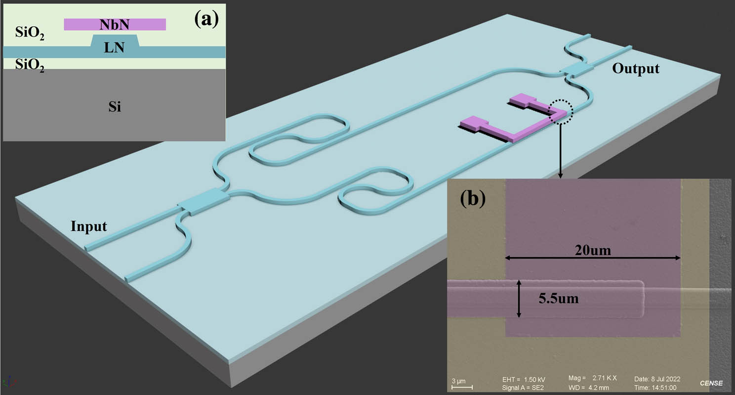
The schematic structure of the TO modulator with an NbN superconducting heater is shown in Fig. 1. The proposed device is fabricated on a 600-nm-thick -cut single crystalline TFLN with 2-µm-thick buried silicon oxide layer sitting on an Si substrate (from NANOLN). Considering both the transmission loss and fabrication processes, the etching depth of the lithium niobate (LN) ridge waveguide is 300 nm, and the width of the ridge waveguide is 1.5 µm[7]. The sidewall angle of the waveguide is approximately 73°. Because the MZI has the advantage of a stabler response over the ring resonator, an asymmetric MZI is used[20]. The modulator is based on an asymmetric multimode interference (MMI) designed with about 550 µm difference, resulting in 2 nm free spectral range (FSR). The MZI has two 3-dB MMI couplers and two straight arms, and one is equipped with an NbN heater that operates as a phase shifter. When an electrode is placed above a waveguide, there will be a more uniform and excellent heat distribution than that when placed beside the waveguide[21]. As the inset of Fig. 1(a), the superconducting NbN heater is positioned 800 nm above the waveguide using a silica spacer to suppress parasitic optical absorption[7]. The inset of Fig. 1(b) shows a false-color scanning electron microscope (SEM) image of the corner area of the NbN heater. The NbN heater on the top layer is covered by light purple, and the silica spacer between the heater and LN waveguide is pale yellow. The size of the heater above the waveguide is . In addition, the width of the NbN connecting wire is 20 µm. Because the critical current is not an intrinsic property of a superconductor, but is dependent upon the size of the conductor, the reduction of sample width results in significant changes in the normal and superconducting state properties[22,23]. To keep the connecting wire in the superconducting state as much as possible, the width of the NbN connecting wire is larger than that of the NbN heater.
![]()
Figure 1.Schematic structure of the TFLN thermo-optical modulator with an NbN superconducting heater. (a) Cross-sectional view of the waveguide and heater (the schematics are not drawn to scale); (b) SEM image of the detail of the heater.
The detailed process flow of the fabrication and packaging procedure is described briefly below. First, the passive LN components were obtained by inductively coupled plasma (ICP) etcher with the Cr mask. Second, 800-nm-thick silica was deposited on the waveguide by plasma-enhanced chemical vapor deposition (PECVD) and was etched by ICP dry etching, except where the metal crosses the waveguide. This silica spacer guarantees that the metal does not cause additional loss. Third, a 100-nm-thick NbN film was deposited using direct-current (DC) reactive magnetron sputtering and lifted off to form the heating electrode. Finally, to facilitate testing at cryogenic temperature, the chip was packaged after the wafer diced into bars and the sides of the bars with input and output ports were polished. A polarization-maintaining (PM) fiber and a single-mode fiber terminated by blocks of optical glass were aligned and glued directly to the input and output interfaces of the chip with cryo-compatible epoxy (GA700H, NTT), respectively. In addition, the electrode pads on the chip and PCB bonding sites on the tube were connected using wire bonding.
3. Measurement
For studying the TO performance of the LN modulator at room temperature and cryogenic temperature, the device was then mounted in a cryostat, as reported previously[24]. The cryostat was equipped with cable feedthroughs for applying electrical signals and fiber feedthroughs: PM fibers for input and single-mode fibers for output for connecting with the modulator. A temperature sensor was installed close to the modulator for measuring the temperature. A tunable laser (Santec TSL-710) with a polarization controller and an optical power meter (Agilent 8163B) were used as an optical input source and an optical output detector, respectively. To study the static characteristics of the LN modulator, an electrical power source (Keithley 2400) was used to apply current to the heater and for thermal tuning. Increasing temperature will increase the refractive index of the LN waveguide and then change the output of the LN modulator[8]. The current, voltage, and transmission were recorded simultaneously when applying the driving voltage on the heater.
The output of the laser source was set at 10 dBm at 1550 nm, and the sweep ranges of the electrical source were 0–30 mA and 0–50 mA for measuring at 293 and 3.45 K, respectively. Figure 2(a) plots the optical transmission versus applied electrical current at both temperatures. From the results, the measured insertion loss is 7.5 and 17 dB (1550 nm) at 293 and 3.45 K, respectively. The above insertion losses come from a polarization controller (0.1 dB), input and output fibers (0.4 dB), and the LN modulator. There is an extra insertion loss in a low-temperature environment, mainly due to the mismatch between the chip and the fiber array caused by the cryogenic temperature[25,26]. As shown in Fig. 2(a), we can see that there are good extinction ratios (ERs) of about 17.2 and 13.4 dB at 293 and 3.45 K, respectively. The total power () can be calculated by the product of the recorded voltage and current. The device’s total power () consumptions are 121 and 246 mW at 293 and 3.45 K, respectively.
![]()
Figure 2.(a) Measured transmission of the modulator under varying applied current; (b) Current-resistance curves measured at 293 and 3.45 K, respectively.
Figure 2(b) plots the applied electrical current versus the total resistance derived from the I-V data at 293 and 3.45 K, respectively. The calculated resistance varies continuously with the current at 293 K but discontinuously with the current at 3.45 K. The above-calculated resistance () includes the resistance of the NbN heater (), the resistance of the NbN connecting wire on chip (), and other resistance connected in series in the test circuit. When measuring at 293 K, the calculated resistance () acts as a normal metal electrode and decreases with increasing temperature. This phenomenon occurs because the NbN superconducting films have a negative temperature coefficient of resistance[23,27]. However, when measuring at 3.45 K, there is a step-up in the calculated resistance () curve. This phenomenon corresponds to the change of the NbN heater and the NbN connecting wire from the superconducting state to the normal state. The resistance of the NbN heater and its connecting wire changes from 0 to 69 Ω, as shown in the inset of Fig. 2(b). This change occurs because the current in the circuit is beyond the superconducting critical current of the NbN at 3.45 K.
Additionally, if we only consider the resistances on the chip (the heating resistor and the NbN connecting wire ) at cryogenic temperatures, we can calculate a net of 48.6 mW at 3.45 K. To reduce power consumption on the chip, the NbN connecting wire should be kept superconducting as much as possible so that the dissipates almost all power. Nevertheless, our proposed device still has very low energy consumption, since it does not always need to heat the heating electrode during the modulation process.
We also investigated the dynamic characteristics of the device at 293 and 3.45 K, respectively. A 2 V square-wave signal with a frequency of 1 kHz and a duty cycle of 0.5 was used as a driven electrical signal on the heater. To ensure that the optical power input to the detector was consistent (), the output power of the laser source was increased when the modulator was measured at 3.45 K. The output of a photodiode (PDA10CF-EC, THORLABS) was recorded using an oscilloscope. Figure 3(a) shows the time response of the TFLN thermo-optical modulator with an NbN superconducting heater at 293 and 3.45 K, respectively. Note that the response magnitude of the proposed device measured at 3.45 K is smaller than that measured at 293 K. A possible reason for this phenomenon is a smaller thermo-optical coefficient at cryogenic temperatures[28,29].
![]()
Figure 3.(a) Time response of the TFLN thermo-optical modulator with an NbN superconducting heater at 293 and 3.45 K, respectively; (b) details of the time response; the red curve is the waveform measured at 293 K, and the blue curve is the waveform measured at 3.45 K.
From the details of the dynamic curve shown in Fig. 3(b), we can calculate the rising and falling time constants, indicating the device’s switching speed. The heating (10%–90%) and cooling (90%–10%) time of the devices at 293 K are 60 and 53 µs [Fig. 3(b-I)], and that of the device at 3.45 K are 22 and 15 µs, respectively [Fig. 3(b-II)]. Because the transition of the NbN heating electrode between the superconducting and the normal states turns the heating and cooling processes from continuous to discontinuous change, the device’s response time at 3.45 K is shorter than that of the device at 293 K.
To study the proposed modulator’s optical performance at room and cryogenic temperatures, the modulator was still mounted in a cryostat, as mentioned above. A broadband optical source replaced the tunable laser, and the output spectrum was monitored with an optical spectrum analyzer (AQ6375B, YOKOGAWA). The device’s transmission spectrum ranged from 1540 to 1560 nm without bias voltage and was measured at 293 and 3.45 K, respectively. The normalized results are shown in Fig. 4. The measured ER at 1550 nm is above 10 dB. A nearly flat spectrum over a wide wavelength range shows a broadband operation in the whole C-band.
![]()
Figure 4.Measured transmission spectra of the device under zero bias at 293 and 3.45 K, respectively.
4. Conclusions
In conclusion, we propose and demonstrate a cryogenic TO modulator in -cut TFLN with an NbN superconducting heater. Replacing the normal metal heating electrode with an NbN superconducting electrode above the TFLN waveguide allows the applied heat to be transferred into the target area discontinuously, thus resulting in faster and power-efficient tuning at cryogenic temperatures. The device’s static and dynamic performance has been characterized at room and cryogenic temperatures. The (10%–90%) rise time and (90%–10%) fall time are 22 and 15 µs at cryogenic temperatures, respectively. The tuning performance can be further improved using other materials with higher TO coefficients and microring structures. The modulator can find its applications in cryogenic optical information processing. It can be integrated monolithically with other photonic elements on the TFLN platform for more functional applications in cryogenic optoelectronics.
References
[16] A. Masood, M. Pantouvaki, G. Lepage, P. Verheyen, J. Van Campenhout, P. Absil, D. Van Thourhout, W. Bogaerts. Comparison of heater architectures for thermal control of silicon photonic circuits. 10th International Conference on Group IV Photonics (GFP), 83(2013).
[24] H. Han, L. Li, P. Yuan, H. Yu, S. Wang, L. You. High-speed optical links for data transfer out of 3.4K to room temperature. IEEE 15th Workshop on Low Temperature Electronics (WOLTE), 1(2022).

Set citation alerts for the article
Please enter your email address
© Copyright 2018-2021 | Chinese Laser Press. All Rights Reserved 沪ICP备15018463号-20