• Journal of Infrared and Millimeter Waves
  • Vol. 42, Issue 5, 574 (2023)
Ming LIU1、*, Cong-Ya YOU1, Jing-Feng LI1, Fa-Ran CHANG2, Tao WEN1, Nong LI2, Peng ZHOU1, Yu CHENG1, and Guo-Wei WANG2、**
Author Affiliations
  • 1North China Research Institute of Electro-optics,Beijing 100015,China
  • 2The State Key Laboratory of Superlattices and Microstructures,Institute of Semiconductors,Chinese Academy of Science,Beijing 100083,China
  • show less
    DOI: 10.11972/j.issn.1001-9014.2023.05.002 Cite this Article
    Ming LIU, Cong-Ya YOU, Jing-Feng LI, Fa-Ran CHANG, Tao WEN, Nong LI, Peng ZHOU, Yu CHENG, Guo-Wei WANG. Research on InAs/GaSb type-II superlattice dual-band long-/long-wavelength infrared photodetector[J]. Journal of Infrared and Millimeter Waves, 2023, 42(5): 574 Copy Citation Text show less
    Schematic of long-/long-wavelength dual-band photodetector architecture and corresponding energy band structure
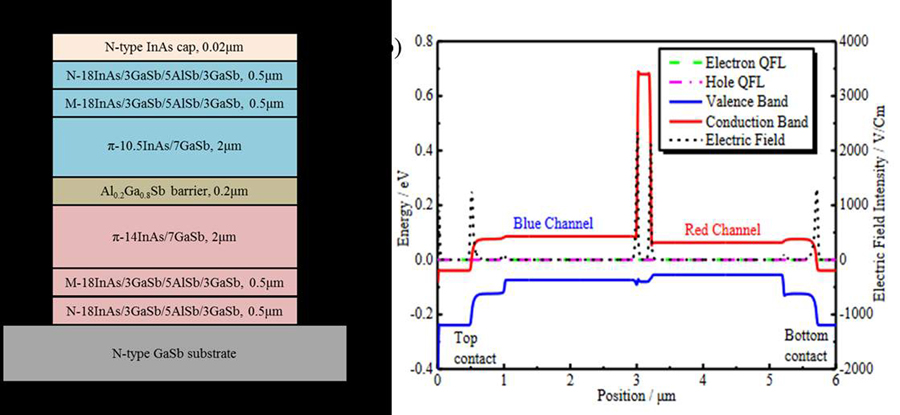
    Fig. 1. Schematic of long-/long-wavelength dual-band photodetector architecture and corresponding energy band structure
    (a)Growth sequence of 10.5 ML InAs/ 7 ML GaSb interface,(b)growth sequence of 14 ML InAs/ 7 ML GaSb interface
    Fig. 2. (a)Growth sequence of 10.5 ML InAs/ 7 ML GaSb interface,(b)growth sequence of 14 ML InAs/ 7 ML GaSb interface
    Surface morphology of long-/long-wavelength dual-band superlattice materials(a)sample #1 and(b)sample #2
    Fig. 3. Surface morphology of long-/long-wavelength dual-band superlattice materials(a)sample #1 and(b)sample #2
    AFM image of long-/long-wavelength dual-band superlattice materials(a)sample #1 and(b)sample #2
    Fig. 4. AFM image of long-/long-wavelength dual-band superlattice materials(a)sample #1 and(b)sample #2
    XRD image of long-/long-wavelength dual-band superlattice
    Fig. 5. XRD image of long-/long-wavelength dual-band superlattice
    (a)Microscopic image of 320×256(30μm)long-/long-wavelength dual-band superlattice photodetector,and(b)scanning electron micrograph of focal pixel array.
    Fig. 6. (a)Microscopic image of 320×256(30μm)long-/long-wavelength dual-band superlattice photodetector,and(b)scanning electron micrograph of focal pixel array.
    Characterization of J-V and RA-V curves
    Fig. 7. Characterization of J-V and RA-V curves
    Spectral response of superlattice dual-band long-/long-wavelength infrared photodetector
    Fig. 8. Spectral response of superlattice dual-band long-/long-wavelength infrared photodetector
    Infrared imagings of dual-band FPA (a) Band-1 channel imaging (b)Band-2 channel imaging
    Fig. 9. Infrared imagings of dual-band FPA (a) Band-1 channel imaging (b)Band-2 channel imaging
    峰位-2级峰-1级峰1级峰2级峰平均值周期厚度设计厚度吻合度
    M结构-4020-202520054035201591.390292.04810.9929
    长长波-5375-2690273554852712.567.889968.27410.9944
    短长波-6795-350031906585334555.052756.53950.9737
    Table 1. The XRD peaks, periodic thicknesses and design match of superlattice
    Ming LIU, Cong-Ya YOU, Jing-Feng LI, Fa-Ran CHANG, Tao WEN, Nong LI, Peng ZHOU, Yu CHENG, Guo-Wei WANG. Research on InAs/GaSb type-II superlattice dual-band long-/long-wavelength infrared photodetector[J]. Journal of Infrared and Millimeter Waves, 2023, 42(5): 574
    Download Citation