
Wei Zheng, Richeng Lin, Lemin Jia, Feng Huang. Vacuum ultraviolet photovoltaic arrays[J]. Photonics Research, 2019, 7(1): 98
- Photonics Research
- Vol. 7, Issue 1, 98 (2019)
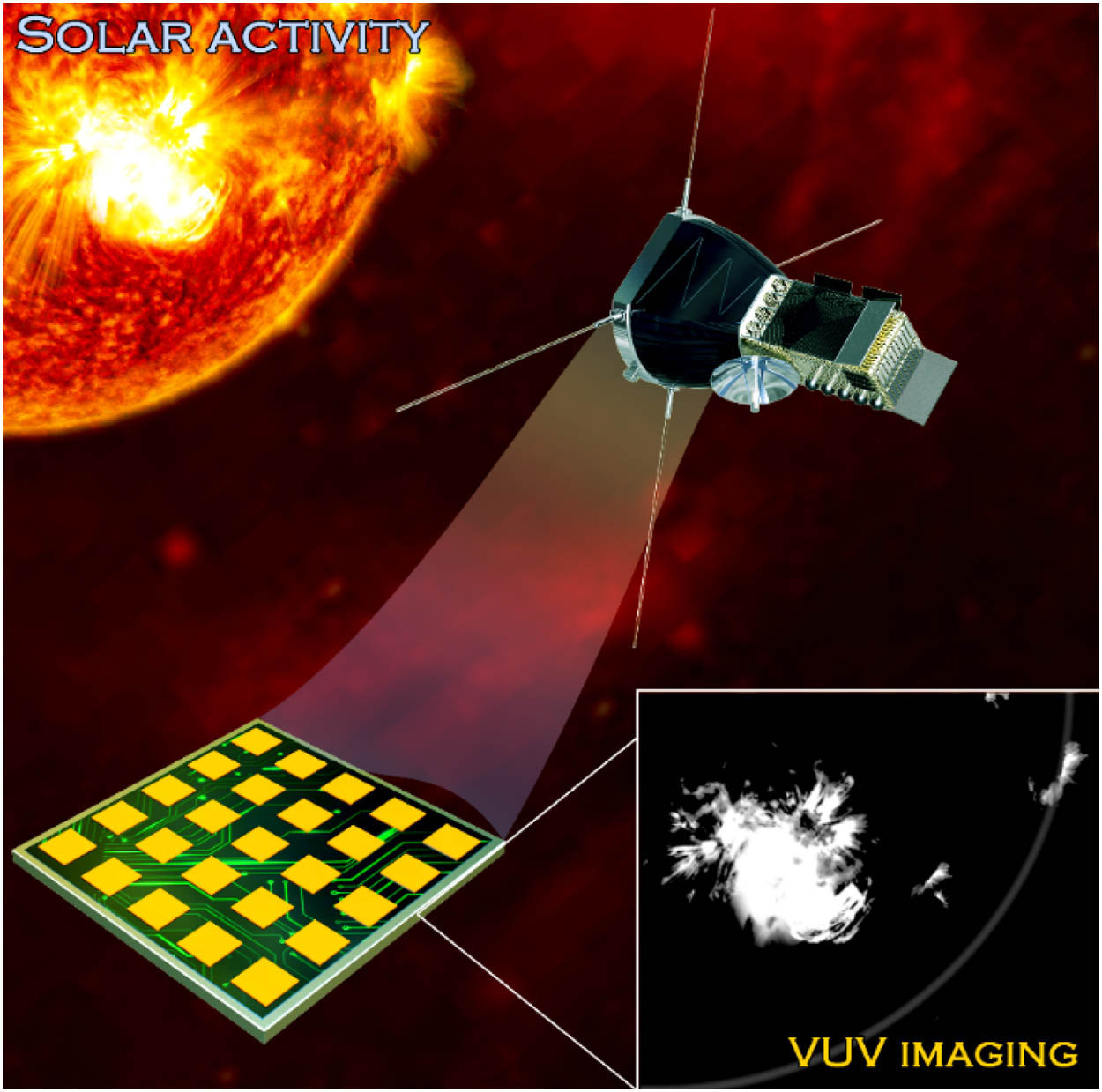
Fig. 1. Schematic illustration of the imaging result of a solar storm using VUV detection technology, which has been sought for a long time. It is obvious that the VUV imaging technology can clearly demonstrate the scene of the solar storm, while the information acquired by traditional imaging technology will be annihilated in the background noise of the Sun.
![Material characterizations of AlN/Si heterostructure. (a) XRD diffraction pattern of the as-grown AlN film on a p-Si substrate. Inset shows the sample. (b) Respective elemental mapping image of Al and N on the surface of the AlN film; (c) cross-sectional TEM image of (001) AlN films on a (111) Si substrate obtained under a near [−2–10] AlN zone axis. The spacing of the atomic layer measured in the image agrees well with the standard lattice constants of Si and AlN crystals. Selected area diffraction pattern of (d) AlN and (e) Si.](/richHtml/prj/2019/7/1/01000098/img_002.jpg)
Fig. 2. Material characterizations of AlN/Si heterostructure. (a) XRD diffraction pattern of the as-grown AlN film on a p-Si substrate. Inset shows the sample. (b) Respective elemental mapping image of Al and N on the surface of the AlN film; (c) cross-sectional TEM image of (001) AlN films on a (111) Si substrate obtained under a near [− 2 – 10
Fig. 3. (a) Schematic diagram of the process of fabricating the VUV photovoltaic arrays; (b) diagram of the VUV imaging test for line array device; (c) result of the device’s line scanning. It is admitted that VUV detectors are supposed to have a sandwich-like vertical structure, within which the photosensitive layer serves as the intermediate layer. The vertical-structure VUV photovoltaic detector also needs to have a VUV transparent conductive material function as the outer window layer to cover the photosensitive layer and to collect photogenerated carriers. Here, we used graphene as the VUV transparent window and constructed HH arrays of p-Gr/AlN/p-Si by means of a wet process and photoetching. It is worth noting that this kind of back-to-back device structure can achieve extremely low dark current and help the device suppress noise. In order to achieve the back-to-back structure of p-i-p, we intentionally performed p-doping on the graphene electrode with the help of nitric acid vapor [6,16]. To obtain high performance of the device, we used Ti/Au and In, respectively, as the contact electrodes for the graphene side and single Si side to achieve a perfect ohmic contact.
Fig. 4. (a) I -V characteristics of a selected photovoltaic unit under an illumination of 185 nm VUV light and dark condition. Inset image is the schematic diagram of the p-Gr/AlN/p-Si HH unit device. (b) Current output characteristics (at zero bias) of the device under 185 nm illumination; (c) noise-voltage density of the detector. We can see that the background noise of the testing device has almost covered an extremely low noise-voltage density. (d) Corresponding band diagram of the device during operation; (e) spectral-dependent photoresponsivity of the device at diffraction wavelengths ranging from 185 to 300 nm; (f) photovoltaic temporal response measured under a 193-nm pulse irradiation. The rise time is 120 ns, and the decay time is 2 ms.
|
Table 1. Figure of Merit Comparisons Between Different Typical Semiconductor-Based VUV Photodetectors

Set citation alerts for the article
Please enter your email address
© Copyright 2018-2021 | Chinese Laser Press. All Rights Reserved 沪ICP备15018463号-20