As one of the ideal tools for monitoring the formation and evolution of solar storms, the vacuum ultraviolet (VUV) detector should have both a fast temporal response and an array structure that enables image formation. Here, by combining a nontraditional graphene processing technique with traditional metal organic chemical vapor deposition epitaxy technology, we created hybrid heterostructure (HH) arrays of p-Gr/AlN/p-Si with VUV photovoltaic response capability and silicon integration potential. The HH arrays not only exhibit ultrafast temporal response (rise time of only 120 ns) and an extremely high ratio of , but also achieve the imaging demonstration of a VUV pattern for the first time. The HH technique provides a possible new path for the development of VUV imaging devices.
1. INTRODUCTION
The large number of coronal ejections produced by solar storms may bring serious attacks on the Earth, which may lead to the short circuit and malfunction of satellites in space and the destruction of the surface power transmission system as well as the communication system [1,2]. For example, the Carrington incident in 1859 witnessed the devastation of human’s first power system caused by a solar storm. In 1989, another small-scale solar storm led to a blackout in Quebec, Canada; in 2003, a huge solar storm paralyzed two satellites, disrupting communications throughout the world [3]. Therefore, in order to make a timely response to solar storms, it is necessary to monitor their generation and evolution.
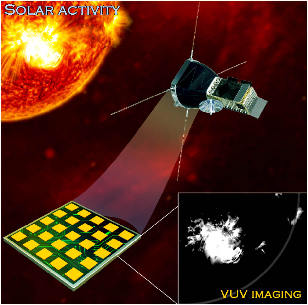
In fact, since vacuum ultraviolet (VUV) (10–200 nm) light is the most suitable information carrier with its lowest sun background noise [2,4], as shown in Fig. 1, solar- and astrophysicists have been working hard over the past 20 years to explore the new-generation semiconductor-based VUV detectors to study the formation of solar storms and the corona [5–11]. Researchers have already made encouraging progress and have even integrated, tested, and applied the new-generation VUV sensors on satellites [2]. However, to achieve real-time monitoring of the dynamic evolution of solar storms, the VUV detector is required to have two of the most critical capabilities: 1) a response speed as fast as possible (close to or even faster than the evolution speed of the monitored solar storm and corona), and 2) the capability of VUV imaging.
Figure 1.Schematic illustration of the imaging result of a solar storm using VUV detection technology, which has been sought for a long time. It is obvious that the VUV imaging technology can clearly demonstrate the scene of the solar storm, while the information acquired by traditional imaging technology will be annihilated in the background noise of the Sun.
To satisfy the first requirement of improving the response speed of the VUV detector, we have made a series of efforts over the past five years. For example, in 2015, we applied micro-/nanostructures to VUV photoconductive detectors [5]. With the help of low-dimensional conductive channels and their inner defect-free advantages, a response speed in milliseconds was achieved. Recently, through the combination of graphene and AlN films, we have produced the first photovoltaic detector that responds to VUV selection, taking a huge leap forward in response rise time to 80 ns, which is to times faster than the previous photoconductive devices [6,7].
Sign up for Photonics Research TOC. Get the latest issue of Photonics Research delivered right to you!Sign up now
To fulfill the second requirement of enabling VUV imaging, here, we further extended the transfer, doping, and cutting-edge technologies of graphene to VUV light detection. We fabricated integrated hybrid heterostructure (HH) arrays of p-Gr/AlN/p-Si on a Si wafer for a total of 20 units, each with a size of μμ. With the line arrays, we have successfully demonstrated VUV photovoltaic imaging. As a result, both the response speed and the imaging capability of the detector meet the requirements as a VUV imaging device. This result attests to the successful progress of a semiconductor VUV device from being a light-intensity detection unit to being an imaging array.
2. EXPERIMENTAL RESULTS AND DISCUSSION
As a matter of fact, AlN is actually one of the most desirable materials for VUV detection [5,6,12], not only because it has exactly the right bandgap of 6.2 eV (corresponding to 200 nm) to realize a perfect VUV selective response, but also because it has strong radiation resistance, which enables long-term stable work in space [9,13]. In order to create a Si-integrated VUV photovoltaic line array detector, we grew a 100-nm epitaxial film of AlN on the p-Si substrate with a (111) surface. The X-ray diffraction (XRD) pattern [Fig. 2(a)] shows a very symmetrical (002), (111) diffraction peak of AlN and Si, demonstrating that AlN film grows along the axis and has good crystal orientation and high crystalline quality, which is also reflected in a high-resolution transmission electron microscope (TEM) image [Fig. 2(c)]. The photo of the scanning electron microscope (SEM) [Fig. 2(b)] and the elemental analysis prove the uniformity of the chemical compositions of the film. The X-ray photoelectron spectroscopy (XPS) pattern further exhibits clearly the Gaussian symmetric emission peaks of and , whose peak positions are close to the ideal values [13]. All the proofs have demonstrated that AlN epitaxial film has relatively pure chemical components and is without other obvious nonideal chemical valences. The characterization mentioned above indicates the high epitaxial quality of AlN film, which results from the related small-lattice mismatch between the (111) plane of Si and the (002) plane of AlN [14].
Figure 2.Material characterizations of AlN/Si heterostructure. (a) XRD diffraction pattern of the as-grown AlN film on a p-Si substrate. Inset shows the sample. (b) Respective elemental mapping image of Al and N on the surface of the AlN film; (c) cross-sectional TEM image of (001) AlN films on a (111) Si substrate obtained under a near [] AlN zone axis. The spacing of the atomic layer measured in the image agrees well with the standard lattice constants of Si and AlN crystals. Selected area diffraction pattern of (d) AlN and (e) Si.
Based on the synthesized high-quality epitaxial film, we used the two-dimensional processing technology of graphene to further fabricate a line array detector consisting of 20 VUV photovoltaic units of μμ [Fig. 3(a)], which has a hybrid heterostructure of p-Gr/AlN/p-Si. This kind of structure has three advantages. First, graphene has a high transmittance of up to 96% for VUV light, which provides the most important VUV transparent conductive window for VUV photovoltaic devices [6,15]. Second, the back-to-back structure of p-i-p can hinder the diffusion of hot carriers and help the device suppress noise. Third, using p-type Si as a substrate is beneficial to the on-chip integration of the device.
Figure 3.(a) Schematic diagram of the process of fabricating the VUV photovoltaic arrays; (b) diagram of the VUV imaging test for line array device; (c) result of the device’s line scanning. It is admitted that VUV detectors are supposed to have a sandwich-like vertical structure, within which the photosensitive layer serves as the intermediate layer. The vertical-structure VUV photovoltaic detector also needs to have a VUV transparent conductive material function as the outer window layer to cover the photosensitive layer and to collect photogenerated carriers. Here, we used graphene as the VUV transparent window and constructed HH arrays of p-Gr/AlN/p-Si by means of a wet process and photoetching. It is worth noting that this kind of back-to-back device structure can achieve extremely low dark current and help the device suppress noise. In order to achieve the back-to-back structure of p-i-p, we intentionally performed p-doping on the graphene electrode with the help of nitric acid vapor [6,16]. To obtain high performance of the device, we used Ti/Au and In, respectively, as the contact electrodes for the graphene side and single Si side to achieve a perfect ohmic contact.
After obtaining the VUV arrays, we used the focus of the quartz object lens to acquire circular VUV spots of a definite diameter [as shown in Fig. 3(b)] and conducted an imaging test. The results show that only the photovoltaic units irradiated by the VUV spots can produce photocurrent output, and the output current value is directly proportional to the intensity of light exposure. When the axis is fixed, we can obtain the current output of the whole line array and perform line imaging, as shown in Fig. 3(c). Further, the device was moved in steps of 200 μm in the direction of the axis, and the line array was subjected to line-to-line current detection every time the device was moved. Ultimately, the picture of the VUV pattern imaging was obtained.
In order to further understand the electrical parameters of various aspects of the device, we selected one photovoltaic unit and conducted comprehensive VUV photoresponse measurements. First of all, the I-V curves of the unit device [Fig. 4(a)] in a dark state and under the illumination of 185 nm VUV light reflect a typical photovoltaic response, which shows an open circuit voltage of 1.4 V. Encouragingly, at an external bias of 0 V, the light/dark current ratio of the device is up to 7 orders of magnitude [Figs. 4(a) and 4(b)], showing an ultrahigh signal-to-noise ratio under the current detection mode [17]. This point is again proved by the extremely low noise voltage density [Fig. 4(c)] of the device.
Figure 4.(a) I-V characteristics of a selected photovoltaic unit under an illumination of 185 nm VUV light and dark condition. Inset image is the schematic diagram of the p-Gr/AlN/p-Si HH unit device. (b) Current output characteristics (at zero bias) of the device under 185 nm illumination; (c) noise-voltage density of the detector. We can see that the background noise of the testing device has almost covered an extremely low noise-voltage density. (d) Corresponding band diagram of the device during operation; (e) spectral-dependent photoresponsivity of the device at diffraction wavelengths ranging from 185 to 300 nm; (f) photovoltaic temporal response measured under a 193-nm pulse irradiation. The rise time is 120 ns, and the decay time is 2 ms.
The mechanism of generating the photovoltaic effect under VUV illumination is shown in Fig. 4(d). When p-type graphene contacts with AlN, the holes of graphene will diffuse to AlN, and the energy band of AlN at the interface will bend up to form a potential energy barrier and produce an internal electric field in the depletion region of the interface. When VUV light passes through graphene into AlN, most of it will be absorbed in the depletion region formed in AlN, resulting in photogenerated electron–hole pairs. Under the influence of the internal electric field, the electrons and holes are separated and move in opposite directions (electrons drift towards AlN, and holes move to graphene). After overcoming the internal resistance of the device, a 1.4 V open circuit voltage is formed between both ends of the device, and VUV photovoltaic response is demonstrated.
We have further evaluated the spectral selectivity of the device. As the spectral-dependent photoresponsivity [Fig. 4(e)] shows, the device has obvious photovoltaic sensitivity to , and its response cutoff wavelength is near 206 nm, which is consistent with the characteristic of spectral absorption of AlN. The photoresponsivity () is an indicator of the photodetector’s ability to detect monochromatic light [18–21], which is defined by the formula , where refers to photocurrent () minus dark current (), refers to the incident optical power density, and means the light-absorbing area of the device. Typically, the photoresponsivity at 185 nm is 5.13 mA/W. The corresponding external quantum efficiency ([22–25], where stands for the Planck constant, refers to light speed, signifies electronic charge, and means the incident light wavelength) is 3.4%.
Since VUV detection is mainly applied to the real-time monitoring of the dynamic process of solar storms, the detector should be endowed with a rapid rise-and-recover response speed [26]. Here, we use a 10 ns pulsed VUV laser of 193 nm to perform a switching temporal-response test on the device. Figure 4(f) shows the result of the detector’s photovoltaic response to a single pulse, and the inset manifests the enlargement of the rising edge. It is encouraging that the rise response time of the device is 120 ns, and the decay time is 2 ms. This relatively long decay time is usually due to the junction capacitance existing inside the device and to the trap states. The response speed of the reported device is 10,000–100,000 times that of the traditional nonimaging photoconductive unit device (see Table 1).
Materials
VUV Light (nm)
Bias (V)
Responsivity (A/W)
Rise Time (s)
Decay Time (s)
Reference
Si
160
—
0.112
[23]
AlN films
180
35
0.0045
<8
<3
[27]
AlN micro/nanowire
190
50
0.39
<0.1
<0.2
[5]
Diamond films
58
1
—
<4
<0.2
[28]
Few-layered h-BN
160
20
2.75
0.0003
0.014
[23]
Two-dimensional MgO
150
4
1.86
<1
<1
[22]
p-Gr/AlN/p-Si
193
0
0.0054
0.00000012
0.002
This work
Table 1. Figure of Merit Comparisons Between Different Typical Semiconductor-Based VUV Photodetectors
In summary, we have reported, to the best of our knowledge, the first imaging-capable integrated VUV photovoltaic arrays with ultrafast response speed, using p-type graphene with unexpected ultrahigh VUV transmittance () as the transparent electrode and high-quality AlN film as the VUV-sensitive layer. In addition, the reported device has displayed nanosecond-level ultrafast temporal response, which can be attributed to the high-quality structure of the device and the high mobility and hole-collection-efficiency of the graphene window. This device combines the traditional metal organic chemical vapor deposition (MOCVD) epitaxy technology with the latest two-dimensional material fabricating technology, which provides a new path for the development of the late-model UV imaging devices.
APPENDIX A: METHODS
AlN Epitaxial Growth
To achieve AlN epitaxial growth, trimethyl aluminum (TMAl) and ammonia () are used, respectively, as the Al source and N source, and hydrogen gas () is used as the carrier gas. After the MOCVD growth parameter reaches the predetermined value and before the AlN film grows, it is necessary to first pass 5 s of TMAl to protect the surface of the Si substrate. The purpose is to prevent the reaction between the Si substrate surface and the . The growth condition of the AlN film is significant, which requires a temperature of 1125°C, an air pressure of 10 kPa, 6000 sccm of flow, and 40 sccm of TMAl flow.
Graphene Array Fabrication
To create graphene arrays, we transferred a large area of graphene to the surface of AlN film through a wet process and built a linear photoresist pattern on the surface of graphene using photoetching techniques. With the help of oxygen plasma, we finally etched out the graphene without photoresist. Then we utilized the method of overlay to construct an electron pattern with a gap of 5 μm and a pad of 400 μm (10 nm Ti and 100 nm Au by electron beam deposition) on the graphene window.
Material Characterization
The equipment for the XRD test was the X-ray diffractometer (PANalytical X’Pert PRO) with α radiation (1 = 0.1 nm). While ZEISS AURIGA’s field emission SEM was used for the SEM test, Tecnai G2 F30 of FEI [300 kV, equipped with high-resolution transmission electron microscopy (HRTEM)] was utilized in the TEM test. In addition, a Thermo Scientific ESCALAB 250 instrument was used in recording the X-ray photoelectron spectra. Also, to carry out the atomic force microscopy (AFM) test, the Dimension Fastscan of Bruker was used.
Device Photoelectric Measurements
In the test of the photovoltaic effect [as shown in Figs. 4(a) and 4(b)], the 185 nm monochromatic light source originates from the quartz-encapsulated low-pressure mercury lamp. The spectral-dependent photoresponse measurement, which adopts a self-assembled “VUV spectral system” [12], is shown in Fig. 4(e). The system contains a 200 W L11798 deuterium lamp (Hamamatsu) and an iHR320 deep-UV monochromator with a diffraction grating blaze at 250 nm (HORIBA). It also utilized a VXUV20A photodetector from Opto Diode Corp. for calibrating monochromatic light power, and the KEYSLEY 6517b for measuring the photocurrent. A self-assembled “VUV pulse system” [12], which contains a 193-nm ArF excimer laser (INC EX5/250 Mini Excimer Laser, GAM LASER) and a 200 M oscilloscope (HDO4022, Teledyne LeCroy), was used to measure the high-speed temporal response [as shown in Fig. 4(f)].