• Chinese Optics Letters
  • Vol. 20, Issue 6, 061302 (2022)
Zhiyi Xuan1、2、3、4, Qingquan Liu1、2、3、4, Zhuangzhuang Cui1、2、4, Songlei Huang2、5, Bo Yang2、3, Chenlu Li1、2、3、4, Shaowei Wang1、2、4、6、*, and Wei Lu1、2、3、4、**
Author Affiliations
  • 1State Key Laboratory of Infrared Physics, Shanghai Institute of Technical Physics, Chinese Academy of Sciences, Shanghai 200083, China
  • 2University of Chinese Academy of Sciences, Beijing 100049, China
  • 3School of Physical Science and Technology, ShanghaiTech University, Shanghai 201210, China
  • 4Shanghai Research Center for Quantum Sciences, Shanghai 201315, China
  • 5State Key Laboratories of Transducer Technology, Shanghai Institute of Technical Physics, Chinese Academy of Sciences, Shanghai 200083, China
  • 6Nantong Academy of Intelligent Sensing, Nantong 226000, China
  • show less
    DOI: 10.3788/COL202220.061302 Cite this Article Set citation alerts
    Zhiyi Xuan, Qingquan Liu, Zhuangzhuang Cui, Songlei Huang, Bo Yang, Chenlu Li, Shaowei Wang, Wei Lu. On-chip short-wave infrared multispectral detector based on integrated Fabry–Perot microcavities array[J]. Chinese Optics Letters, 2022, 20(6): 061302 Copy Citation Text show less
    (a) Schematic diagram of the FP microcavities array directly integrated on an InGaAs detector. (b) Simulated spectra of 16 FP microcavities array directly integrated on the InGaAs FPA.
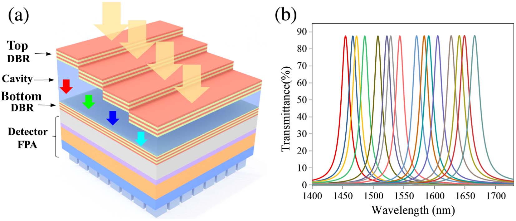
    Fig. 1. (a) Schematic diagram of the FP microcavities array directly integrated on an InGaAs detector. (b) Simulated spectra of 16 FP microcavities array directly integrated on the InGaAs FPA.
    Fabrication process of on-chip InGaAs multispectral detector. (a) The InGaAs FPA. (b) The bottom DBR and cavity layer are deposited on the InGaAs FPA. (c) The cavity layer is processed with UV lithography and ICP etching. (d) The top DBR is deposited on the processed cavity layer and forms 16 different FP microcavities.
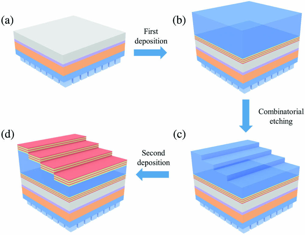
    Fig. 2. Fabrication process of on-chip InGaAs multispectral detector. (a) The InGaAs FPA. (b) The bottom DBR and cavity layer are deposited on the InGaAs FPA. (c) The cavity layer is processed with UV lithography and ICP etching. (d) The top DBR is deposited on the processed cavity layer and forms 16 different FP microcavities.
    (a) Cross-section SEM image of a representative monolithic integrated FP cavity with structure of (LH)32.37L(HL)3, where H is the Si layer, and L is the SiO2 layer. (b) The picture of the fabricated 16-channel multispectral detector chip with ROIC of the size about 2 mm2. (c) The 64 × 64 pixels InGaAs detector FPA. (d) The 16-channel FP microcavities array, which is monolithically integrated with the detector chip.
    Fig. 3. (a) Cross-section SEM image of a representative monolithic integrated FP cavity with structure of (LH)32.37L(HL)3, where H is the Si layer, and L is the SiO2 layer. (b) The picture of the fabricated 16-channel multispectral detector chip with ROIC of the size about 2 mm2. (c) The 64 × 64 pixels InGaAs detector FPA. (d) The 16-channel FP microcavities array, which is monolithically integrated with the detector chip.
    (a) Schematic diagram of the InGaAs FPA response spectrum test system. (b) The measured response spectrum of the standard detector. (c) The measured response spectra of the 16-channel multispectral detector.
    Fig. 4. (a) Schematic diagram of the InGaAs FPA response spectrum test system. (b) The measured response spectrum of the standard detector. (c) The measured response spectra of the 16-channel multispectral detector.
    Zhiyi Xuan, Qingquan Liu, Zhuangzhuang Cui, Songlei Huang, Bo Yang, Chenlu Li, Shaowei Wang, Wei Lu. On-chip short-wave infrared multispectral detector based on integrated Fabry–Perot microcavities array[J]. Chinese Optics Letters, 2022, 20(6): 061302
    Download Citation