
He Guan, Cheng-Yu Jiang, Shao-Xi Wang. Effect of annealing temperature on interfacial and electrical performance of Au–Pt–Ti/HfAlO/InAlAs metal–oxide–semiconductor capacitor[J]. Chinese Physics B, 2020, 29(9):
- Chinese Physics B
- Vol. 29, Issue 9, (2020)
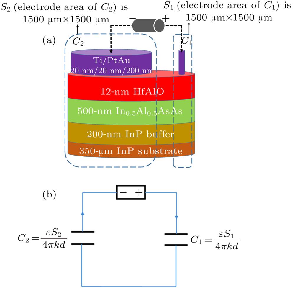
Fig. 1. (a) Structure diagram of MOS capacitor, and (b) equivalent circuit of the MOS capacitor.
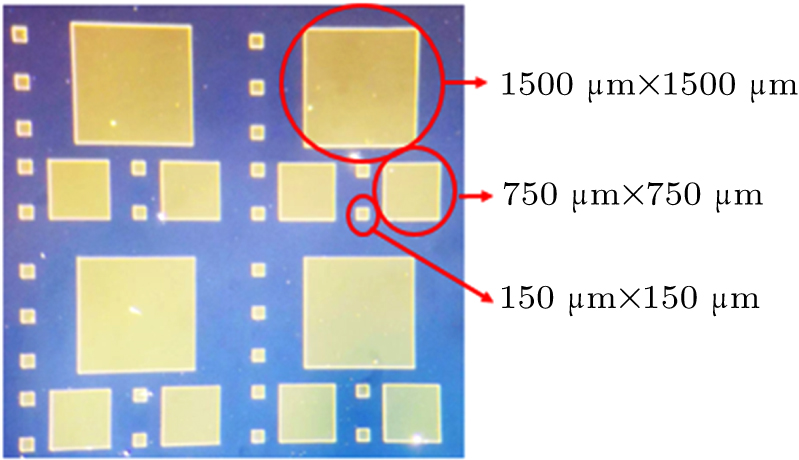
Fig. 2. Photograph of Ti/Pt/Au metal electrode.
Fig. 3. AFM line scan of HfAlO/InAlAs surfaces of samples annealed at (a) 330 °C, (b) 380 °C, (c) 430 °C, and (d) 480 °C.
Fig. 4. RMS roughness value versus PDA temperature of the samples.
Fig. 5. XPS results after annealing processing of (a) As 3d, (b) Hf 4f, (c) Al 2p, (d) In 3d2/5.
Fig. 6. Interfacial oxide content under annealing temperatures of 280, 380, and 480 °C.
Fig. 7. The C –V characteristics of HfAlO/InAlAs MOS-capacitor at different annealing temperatures.
Fig. 8. Interfacial state density (D it) of HfAlO/InAlAs MOS-capacitor with different annealing temperatures. (E t – E i) indicates the distance from energy level of interface trap state (E t) to intrinsic Fermi level (E i).
Fig. 9. Leakage current densities of HfAlO/InAlAs MOS-capacitor at different annealing temperatures.
|
Table 1. Electrical parameters extracted from C–V measurements for HfAlO/InAlAs MOS-capacitor with different annealing temperatures.


Set citation alerts for the article
Please enter your email address

© Copyright 2018-2021 | Chinese Laser Press. All Rights Reserved 沪ICP备15018463号-20