Abstract
The tilted energy band in the multiple quantum wells (MQWs) arising from the polarization effect causes the quantum confined Stark effect (QCSE) for [0001] oriented III-nitride-based near ultraviolet light-emitting diodes (NUV LEDs). Here, we prove that the polarization effect in the MQWs for NUV LEDs can be self-screened once the polarization-induced bulk charges are employed by using the alloy-gradient InxGa1-xN quantum barriers. The numerical calculations demonstrate that the electric field in the quantum wells becomes weak and thereby flattens the energy band in the quantum wells, which accordingly increases the spatial overlap for the electron-hole wave functions. The polarization self-screening effect is further proven by observing the blueshift for the peak emission wavelength in the calculated and the measured emission spectra. Our results also indicate that for NUV LEDs with a small conduction band offset between the quantum well and the quantum barrier, the electron injection efficiency for the proposed structure becomes low. Therefore, we suggest doping the proposed quantum barrier structures with Mg dopants.Compared with the conventional fluorescence-based light emitters, III-nitride-based light-emitting diodes (LEDs) possess many excellent advantages of being environmentally-friendly, small size, long lifetime, and high wall-plug efficiency (WPE)[1]; thus they are broadly used in illumination and communication[2,3]. As one member of the nitride LED family, LEDs with an emission spectrum in the near ultraviolet region (i.e., NUV LEDs) are widely applied in photolithography, agent detection, UV curing, etc., and thus have attracted extensive research efforts[4]. Therefore, it is very important to understand the important factors that influence the quantum efficiency for NUV LEDs. As is well known, besides the carrier injection, the polarization-induced electric field is another challenging issue for [0001] oriented nitride-based LEDs[5]. There have been effective designs proposed to reduce the electron leakage, and some typical approaches include making electrons less energetic[6], increasing the blocking effect for the quantum barriers and p-type electron blocking layer (p-EBL)[7,8], and reducing the electron accumulation at the last quantum barrier/p-EBL interface[9]. Another bottleneck for nitride LEDs lies on the hole injection efficiency. Considering the low mobility for holes, we have to make holes more energetic[10], since by doing so, the blocking effect caused by the quantum barriers and the p-EBL can be mitigated. The poor hole injection efficiency is also the consequence of the inadequate hole concentration in the hole supplier layer. Hence, the AlGaN/GaN superlattice doping and three-dimensional hole gas (3DHG) are proposed to improve the hole concentration in the supplier layer[11,12]. Owing to the intrinsic characteristic of the wurtzite structure, [0001] oriented III-nitride-based heterojunctions strongly suffer from the polarization effect, which bends the energy band in the multiple quantum wells (MQWs). On one hand, the tilted energy band spatially separates the electron-hole wave function, thereby reducing the radiative recombination rate, which is known as quantum confined Stark effect (QCSE)[5], and on the other hand, the tilted energy band inevitably increases the carrier density in the MQWs and then aggravates the Auger recombination, whose rate equals the value of ( and denote the Auger recombination coefficient and the carrier density, respectively)[13]. To mitigate the polarization effect within the MQWs, a widely accepted approach is to fabricate LEDs on the nonpolar and semipolar substrates[14,15]. For LEDs grown along the [0001] orientation, the QCSE can be mitigated by adopting polarization matched AlGaInN quantum barriers or Si-doped quantum barriers[16–19]. Moreover, Zhang et al. reveal the importance of the ionized Si dopants in screening the polarization charges in the MQWs[20]. This concept is further proven by Kim et al.[21]. Zhang et al. utilize the polarization-induced bulk charges to effectively weaken the polarization effect for blue LEDs via linearly increasing or decreasing the InN component of the quantum barriers, i.e., polarization self-screening effect[22]. Thus, the polarization effect in the MQWs has been extensively investigated for In-rich InGaN/GaN-based blue and green LEDs[14–18,20–23]. However, with the InN composition for InGaN quantum wells decreasing, the polarization effect within the quantum wells and the approaches to screen the polarization are less studied for NUV LEDs. Meanwhile, the impact of the polarization-screened active region on the carrier distribution is still unclear for NUV LEDs. Hence, we investigate the polarization self-screening effect for NUV LEDs in this work both numerically and experimentally. The polarization-induced bulk charges can be achieved by varying the alloy component for the ternary III-nitride compound[8,22]. For the proof of the polarization self-screening effect, we linearly increase the InN composition of the -based quantum barriers along the [0001] orientation for NUV LEDs. Our results indicate the polarization-induced electric field in the MQWs can be effectively reduced by the polarization-induced bulk charges generated in the alloy-gradient quantum barriers. Meanwhile, the energy bandgap for the quantum barriers shrinks, and thus the hole transport is simultaneously enhanced in the active region.
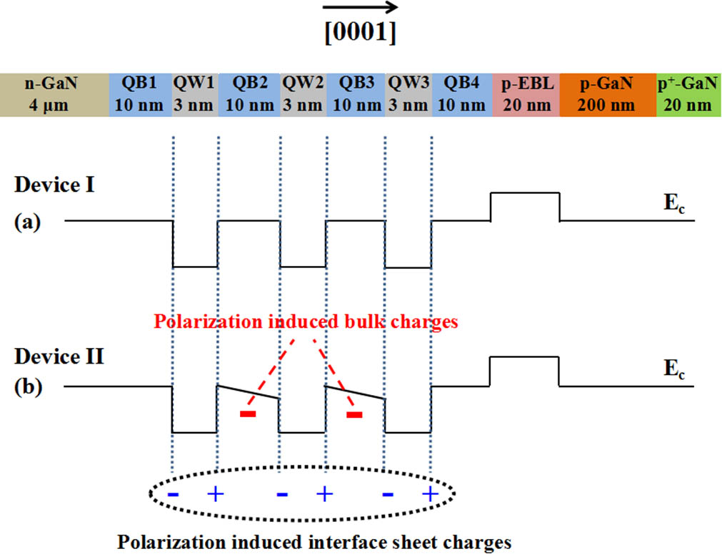
In order to investigate the polarization self-screening effect for NUV LEDs, two device structures [see Figs. 1(a) and 1(b)] are designed and then grown on the c-plane sapphire substrate by the metal organic chemical vapor deposition (MOCVD) technology. Trimethylgallium (TMGa), trimethylaluminum (TMAl), trimethylindium (TMIn), and ammonia () serve as precursors for the Ga, Al, In, and N sources, respectively. The diluted and the are used as the precursors for the Si and Mg dopants, respectively. The carrier gases are and . The initial layer on the sapphire substrate is the GaN nucleation layer, for which the thickness is 20 nm. The following layer is the unintentionally doped GaN (u-GaN) layer with the thickness of 2 μm. The electron supplier layer is a 4 μm thick n-GaN layer with the electron concentration of . The active region consists of a three-period 3 nm thick quantum well (QW) and a 10 nm thick quantum barrier (QB). The two devices (i.e., Device I and Device II) are of the same structure except for the quantum barriers. The QB material for Device I is GaN. For Device II, the InN composition of QB2 and QB3 has been linearly increased from 0 to 0.03, while the others (i.e., QB1 and QB4) also utilize GaN as the QB [see Fig. 1(b)]. Then, the active region is capped with a p-type layer serving as the p-EBL, the thickness of which is 20 nm. The next layer is a 200 nm thick p-GaN layer, which supplies holes for NUV LEDs. The hole concentration for the p-EBL and the p-GaN layer is . Finally, a 20 nm thick p+-GaN layer is employed serving as the ohmic contact. Additionally, Figs. 1(a) and 1(b) also present the polarization-induced interface sheet charge profiles for the investigated devices. Because the InN composition of the QB2 and QB3 is linearly increased along the [0001] orientation, the negative polarization-induced bulk charges are generated therein [see Fig. 1(b)]. The generation mechanism for the polarization-induced bulk charges can be found in Ref. [22].

Figure 1.Schematic conduction band diagrams for: (a) Device I; (b) Device II, in which the distributions of polarization-induced interface sheet charges and the polarization-induced bulk charges are also shown. represents the conduction band.
To in-depth explain the underlying device physics regarding the polarization self-screening effect in the MQWs, numerical calculations are conducted with the aid of the Crosslight APSYS[5,8,10,19,20,22]. The drift-diffusion equations, Schrödinger and Poisson’s equations, are involved and computed self-consistently with appropriate boundary conditions. The nonradiative recombination in the active region is also considered in our calculations by setting the Auger recombination coefficient and the Shockley–Read–Hall (SRH) recombination lifetime to and [24,25], respectively. The band offset ratio (/) for InGaN/GaN QWs is set to 70:30[26]. The value of the polarization-induced charge density in our model, which is calculated by referring to the method proposed by Fiorentini et al.[27], reflects the intensity of the spontaneous and piezoelectric polarizations. Considering the crystalline relaxation in the experiment, we set the polarization level to 0.4, which means 0.4 of the theoretical polarization charges are considered in our calculation while the others are released by the crystalline relaxation (i.e., generating dislocations)[5,8,10,20,22,27]. Specifically, the negative polarization-induced bulk charge density in QB2 and QB3 for Device II is , which is calculated by [22], where represents the polarization density, represents the InN composition, and represents the thickness of the gradient QB. Other parameters of III-nitride-based semiconductors can be found in Ref. [28].
Sign up for Chinese Optics Letters TOC. Get the latest issue of Chinese Optics Letters delivered right to you!Sign up now
We first present the electric field profiles for Devices I and II in Fig. 2(a) at the current injection level of . Obviously, we can see that the overall electric field intensity in the QB2 and QB3 for Device II decreases when compared to that for Device I. We can also observe that the electric field in the QWs for Device II is significantly reduced. The reduced electric field in the QB2 and QB3 is mainly ascribed to the truth that the positive polarization-induced sheet charges can be efficiently compensated by the negative polarization-induced bulk charges generated in the QB with increased InN composition therein, i.e., the polarization self-screening effect for the MQWs. The reduced electric field intensity in the QWs can also be explained by the equation [22], in which and represent the electric field profiles in the QB and the QW, respectively. and are the thickness for the quantum barrier and the quantum well, respectively. Hence, is closely related to and a reduced can bring about a small provided that and are unchanged. The electric field intensity in the QWs also influences the energy band alignment. For the purpose of demonstration, we then selectively illustrate the conduction band and the valence band profiles of QW2 for the studied devices in Figs. 2(b) and 2(c), respectively. As the electric field intensity in QW2 for Device II reduces, both the conduction band and the valence band are less tilted than that for Device I, such that the conduction band of the QW for Device II is bent upward by 14.75 meV and the valence band of the QW for Device II is bent downward by 14.75 meV. The less tilted energy band of the QW can increase the spatial overlap for the carrier wave functions , which are 66.2% and 70.0% of QW2 for Devices I and II, respectively.
Figure 2.(a) Electric field profiles, (b) combined conduction band profiles, and (c) combined valence band profiles for Devices I and II. Data are collected at . and are both 14.75 meV.
As shown in Figs. 2(a), 2(b), and 2(c), the reduced makes the energy band of the QW less tilted, which can increase the emission energy, thereby causing a blueshift for the peak emission wavelength. Then, we present the calculated and the measured emission spectra at different current injection levels in Figs. 3(a) and 3(b), respectively. Figure 3 demonstrates that the evolutional tendency for the calculated emission spectra is consistent with the experimental ones, such that the peak emission wavelength shows the blueshift for Device II when compared to Device I. The observed blueshift for the emission wavelength strongly proves that the polarization-induced electric field in the MQWs for Device II is efficiently self-screened by the polarization-induced bulk charges generated in the QBs.
Figure 3.(a) Calculated and (b) measured EL spectra for Devices I and II at the currents of and , respectively.
Next, Fig. 4(a) further shows the calculated peak emission wavelength and the light output power (LOP) for the investigated devices in terms of the current injection levels. The measured ones are shown in Fig. 4(b). We can clearly see that both the calculated and the measured peak emission wavelengths for Device II are shorter than that for Device I at different current injection levels, which further certifies that the electric field in the MQWs has been significantly reduced by the polarization-induced bulk charges in the QBs. Figure 4(a) also shows that, as the current injection level increases, the calculated peak emission wavelengths both for Devices I and II decrease, which is because the electric field in the MQWs is screened by the injected nonequilibrium carriers. The inset for Fig. 4(a) selectively demonstrates the in terms of the injection current density of QW2 for the two devices, which is enhanced for Device II. The improved well proves the screened polarization level in the QWs. Moreover, the energy band filling effect that easily occurs at a high injection current level also leads to the blueshift for the emission wavelength[29]. Note, to insightfully investigate the polarization self-screening effect in the MQWs, we purposely do not consider the self-heating effect in our physical models. Nevertheless, the measured peak emission wavelength tends to increase with the increasing current injection level and the generated redshift for the peak emission wavelength is mainly due to the self-heating effect[30], which also accounts for the decreased LOP for the two devices at the high current density [see Fig. 4(b)]. Note, the reduced electric field in the MQWs can give rise to the increased electron-hole wave function overlap, which is beneficial to improve the LOP. Surprisingly, according to Figs. 3 and 4, both the calculated and the measured EL intensity and LOP for Device II are lower than that for Device I, which will be analyzed in detail as follows.
Figure 4.(a) Numerically computed and (b) experimentally measured light output power and peak emission wavelengths in terms of the current injection levels. Inset for Fig. 4(a) presents the calculated electron-hole overlap level in QW2 at different injection current density levels.
The LOP is also affected by the carrier concentration within the MQWs. Hence, we show the distribution profiles for holes and electrons across the active region in Figs. 5(a) and 5(b), respectively. As is well known, the hole injection efficiency can be significantly decreased when Si-doped QBs are adopted[19]. Fortunately, Fig. 5(a) shows that the hole blocking effect can be remarkably mitigated in our proposal and the holes for Device II are able to travel into the deepest quantum well (i.e., QW1). The improved hole distribution across the active region arises from the reduced effective barrier height in the valence band when quantum barriers are utilized. Nevertheless, the quantum barriers also simultaneously reduce the effective conduction band barrier height and thus weaken the confinement capability for electrons, more electrons tend to escape from the first and second quantum wells, and are injected into the last quantum well close to the p-EBL, as shown in Fig. 5(b). Meanwhile, the least hole concentration in the last quantum well [see Fig. 5(a)] cannot effectively recombine with electrons, which further increases the electron leakage [see inset for Fig. 5(b)]. Therefore, the reduced electron injection efficiency accounts for the weaker EL intensity and lower LOP for Device II. Our results let us realize that InGaN/GaN-based NUV LEDs have a smaller conduction band offset when compared with InGaN/GaN-based blue and green LEDs[31,32], and we shall increase the electron injection efficiency by, e.g., reducing the electron kinetic energy[6], increasing the conduction band barrier height for the MQWs[7].
Figure 5.(a) Hole concentration profiles and (b) electron concentration profiles in the MQWs for Devices I and II at the current level of . Inset for Fig. 5(b) shows the normalized electron current density for Devices I and II at the current level of .
Here, we suggest an easy way to improve the electron injection, i.e., doping the quantum barriers for Device II with Mg dopants, so that the Mg-doped quantum barriers are able to enhance the confinement capability for electrons by increasing the effective conduction band barrier height[33]. Therefore, we further show the optical power and the electron current density for Device III that has the Mg-doped quantum barriers (Mg dosage level is set to ). The comparison between Devices I and III shows that the optical power for Device III improves [see Fig. 6(a)]. The enhanced optical power for Device III is attributed to the suppressed electron leakage according to Fig. 6(b).
Figure 6.(a) Numerically computed light output power and (b) normalized electron current density for Devices I, II, and III. The electron current density is collected at .
In summary, polarization self-screening has been proposed for [0001] oriented NUV LEDs both theoretically and experimentally. The essence of the polarization self-screening effect is realized once the alloy component in the ternary quantum barriers is linearly varied, which will then generate the polarization-induced bulk charges and function as the ionized dopants in the Si-doped quantum barriers. The polarization self-screening effect is further proven by linearly increasing the InN composition along the [0001] growth orientation of the InGaN quantum barriers for NUV LEDs. The reduced electric field intensity for the proposed structure is observed, which helps to flatten the energy band for the quantum wells and thus increases the overlap level of the electron-hole wave function. The polarization self-screening effect for the proposed MQW structure is further proven by observing the blueshift for the peak emission wavelength. The MQW structure for the proposed NUV LED also favors the hole transport. We also point out that the electron injection efficiency shall be increased by, e.g., reducing the electron kinetic energy[6], enhancing the confinement capability of the conduction band for NUV LEDs[7]. Our results show that doping the quantum barriers with Mg dopants of the proper dosage level and/or proper doped position is promising to suppress the electron leakage and improve electron injection efficiency. Therefore, this work has provided further physical understanding for InGaN/GaN NUV LEDs. We also believe the proposed approach also enables the polarization screening effect and the improved hole injection for AlGaN-based deep ultraviolet light-emitting diodes. Thus, this work is very useful for the III-nitride optoelectronic community.
References
[1] E. F. Schubert, J. K. Kim. Science, 308, 1274(2005).
[2] Z. T. Li, H. Y. Wang, B. H. Yu, X. R. Ding, Y. Tang. Chin. Opt. Lett., 15, 042301(2017).
[3] J. B. Luo, Y. Tang, H. P. Jia, Q. W. Zhu, W. Xue. Chin. Opt. Lett., 14, 120604(2016).
[4] M.-K. Kwon, Il.-K. Park, J.-Y. Kim, J.-O. Kim, B. Kim, S.-J. Park. IEEE Photonics Technol. Lett., 19, 1880(2007).
[5] Z.-H. Zhang, Y. Zhang, W. Bi, H. V. Demir, X. W. Sun. Phys. Status Solidi A, 213, 3078(2016).
[6] X. Ni, X. Li, J. Lee, S. Liu, V. Avrutin, Ü. Özgür, H. Morkoç, A. Matulionis. J. Appl. Phys., 108, 033112(2010).
[7] G. Liu, J. Zhang, C. K. Tan, N. Tansu. IEEE Photonics J., 5, 2201011(2013).
[8] Z.-H. Zhang, W. Liu, Z. Ju, S. T. Tan, Y. Ji, X. Zhang, L. Wang, Z. Kyaw, X. W. Sun, H. V. Demir. Appl. Phys. Lett., 104, 251108(2014).
[9] D. S. Meyaard, G.-B. Lin, M. Ma, J. Cho, E. F. Schubert, S.-H. Han, M.-H. Kim, H. Shim, Y. S. Kim. Appl. Phys. Lett., 103, 201112(2013).
[10] Z.-H. Zhang, W. Liu, S. T. Tan, Y. Ji, L. Wang, B. Zhu, Y. Zhang, S. Lu, X. Zhang, N. Hasanov, X. W. Sun, H. V. Demir. Appl. Phys. Lett., 105, 153503(2014).
[11] I. D. Goepfert, E. F. Schubert, A. Osinsky, P. E. Noms, N. N. Faleev. J. Appl. Phys., 88, 2030(2000).
[12] L. Zhang, X. C. Wei, N. X. Liu, H. X. Lu, J. P. Zeng, J. X. Wang, Y. P. Zeng, J. M. Li. Appl. Phys. Lett., 98, 241111(2011).
[13] E. Kioupakis, P. Rinke, K. T. Delaney, C. G. Van de Walle. Appl. Phys. Lett., 98, 161107(2011).
[14] S.-C. Ling, T.-C. Lu, S.-P. Chang, J.-R. Chen, H.-C. Kuo, S.-C. Wang. Appl. Phys. Lett., 96, 231101(2010).
[15] A. E. Romanov, T. J. Baker, S. Nakamura, J. S. Speck. J. Appl. Phys., 100, 023522(2006).
[16] J.-Y. Chang, Y. K. Kuo. Opt. Lett., 37, 1574(2012).
[17] M. F. Schubert, J. Xu, J. K. Kim, E. F. Schubert, M. H. Kim, S. Yoon, S. M. Lee, C. Sone, T. Sakong, Y. Park. Appl. Phys. Lett., 93, 041102(2008).
[18] V. Fiorentini, F. Bernardini, F. D. Sala, A. D. Carlo, P. Lugli. Phys. Rev. B, 60, 8849(1999).
[19] K. K. Tian, Q. Chen, C. S. Chu, M. Q. Fang, L. P. Li, Y. H. Zhang, W. G. Bi, C. Q. Chang, Z.-H. Zhang, J. N. Dai. Phys. Status Solidi RRL, 12, 1700346(2018).
[20] Z.-H. Zhang, S. T. Tan, Z. Ju, W. Liu, Y. Ji, Z. Kyaw, Y. Dikme, X. W. Sun, H. V. Demir. J. Disp. Technol., 9, 226(2013).
[21] D. Y. Kim, G.-B. Lin, S. Hwang, J. H. Park, D. Meyaard, E. F. Schubert, H.-Y. Ryu, J. K. Kim. IEEE Photonics J., 7, 1300209(2015).
[22] Z.-H. Zhang, W. Liu, Z. Ju, S. T. Tan, Y. Ji, Z. Kyaw, X. Zhang, L. Wang, X. W. Sun, H. V. Demir. Appl. Phys. Lett., 104, 243501(2014).
[23] R. Sharma, P. M. Pattison, H. Masui, R. M. Farrell, T. J. Baker, B. A. Haskell, F. Wu, S. P. DenBaars, J. S. Speck, S. Nakamura. Appl. Phys. Lett., 87, 231110(2005).
[24] M. Meneghini, N. Trivellin, G. Meneghesso, E. Zanoni, U. Zehnder, B. Hahn. J. Appl. Phys., 106, 114508(2009).
[25] J. Piprek, S. Li. Opt. Quantum Electron., 42, 89(2011).
[26] J. Piprek. Phys. Status Solidi A, 207, 2217(2010).
[27] V. Fiorentini, F. Bernardini, O. Ambacher. Appl. Phys. Lett., 80, 1204(2002).
[28] I. Vurgaftman, J. R. Meyer. J. Appl. Phys., 94, 3675(2003).
[29] J.-C. Wang, C.-H. Fang, Y.-F. Wu, W.-J. Chen, D.-C. Kuo, P.-L. Fan, J.-A. Jiang, T.-E. Nee. J. Lumin., 132, 429(2012).
[30] T.-C. Wang, H.-C. Kuo, Z.-H. Lee, C.-C. Chuo, M.-Y. Tsai, C.-E. Tsai, T.-D. Lee, T.-C. Lu, J. Chi. J. Cryst. Growth, 287, 582(2006).
[31] K. Zhou, M. Ikeda, J. Liu, S. Zhang, D. Li, L. Zhang, J. Cai, H. Wang, H. B. Wang, H. Yang. Appl. Phys. Lett., 105, 173510(2014).
[32] S.-H. Park, Y.-T. Moon, J. Lee, H. Kwon, J. Park, D. Ahn. Phys. Status Solidi A, 208, 195(2011).
[33] S. H. Han, C. Y. Cho, S. J. Lee, T. Y. Park, T. H. Kim, S. H. Park, S. W. Kang, J. W. Kim, Y. C. Kim, S. J. Park. Appl. Phys. Lett., 96, 051113(2010).