• Photonics Research
  • Vol. 9, Issue 5, 749 (2021)
Xiao Hu1、2, Dingyi Wu2, Hongguang Zhang1, Weizhong Li1、2, Daigao Chen1、2, Lei Wang1、2, Xi Xiao1、2、*, and Shaohua Yu1、2
Author Affiliations
  • 1National Information Optoelectronics Innovation Center, China Information and Communication Technologies Group Corporation (CICT), Wuhan 430074, China
  • 2State Key Laboratory of Optical Communication Technologies and Networks, China Information and Communication Technologies Group Corporation (CICT), Wuhan 430074, China
  • show less
    DOI: 10.1364/PRJ.417601 Cite this Article Set citation alerts
    Xiao Hu, Dingyi Wu, Hongguang Zhang, Weizhong Li, Daigao Chen, Lei Wang, Xi Xiao, Shaohua Yu. High-speed and high-power germanium photodetector with a lateral silicon nitride waveguide[J]. Photonics Research, 2021, 9(5): 749 Copy Citation Text show less

    Abstract

    Up to now, the light coupling schemes of germanium-on-silicon photodetectors (Ge-on-Si PDs) could be divided into three main categories: (1) vertical (or normal-incidence) illumination, which can be from the top or back of the wafer/chip, and waveguide-integrated coupling including (2) butt coupling and (3) evanescent coupling. In evanescent coupling the input waveguide can be positioned on top, at the bottom, or lateral to the absorber. Here, to the best of our knowledge, we propose the first concept of Ge-on-Si PD with double lateral silicon nitride (Si3N4) waveguides, which can serve as a novel waveguide-integrated coupling configuration: double lateral coupling. The Ge-on-Si PD with double lateral Si3N4 waveguides features uniform optical field distribution in the Ge region, which is very beneficial to improving the operation speed for high input power. The proposed Ge-on-Si PD is comprehensively characterized by static and dynamic measurements. The typical internal responsivity is evaluated to be 0.52 A/W at an input power of 25 mW. The equivalent circuit model and theoretical 3 dB opto-electrical (OE) bandwidth investigation of Ge-on-Si PD with lateral coupling are implemented. Based on the small-signal (S21) radio-frequency measurements, under 4 mA photocurrent, a 60 GHz bandwidth operating at -3 V bias voltage is demonstrated. When the photocurrent is up to 12 mA, the 3 dB OE bandwidth still has 36 GHz. With 1 mA photocurrent, the 70, 80, 90, and 100 Gbit/s non-return-to-zero (NRZ) and 100, 120, 140, and 150 Gbit/s four-level pulse amplitude modulation clear openings of eye diagrams are experimentally obtained without utilizing any offline digital signal processing at the receiver side. In order to verify the high-power handling performance in high-speed data transmission, we investigate the eye diagram variations with the increase of photocurrents. The clear open electrical eye diagrams of 60 Gbit/s NRZ under 20 mA photocurrent are also obtained. Overall, the proposed lateral Si3N4 waveguide structure is flexibly extendable to a light coupling configuration of PDs, which makes it very attractive for developing high-performance silicon photonic integrated circuits in the future.

    1. INTRODUCTION

    Silicon photonics is a fascinating technology to realize large-scale electronics-photonics integration on a chip with low cost, high bandwidth, large volume, high energy efficiency, and complementary metal-oxide semiconductor (CMOS) compatibility [15]. Silicon photonics has been proving its great worth in data centers, long-haul telecommunication, integrated quantum communication, integrated microwave photonics, artificial intelligence (AI), and high-performance computers [2,48].

    One of the key building blocks of silicon photonics is photodetectors (PDs) that convert high-speed optical signals to electrical signals [9,10]. However, the intrinsic properties of silicon (Si), an indirect band-gap semiconductor with a band-gap energy of 1.1 eV which is transparent in the near-IR wavelength band (1.3–1.55 μm), make it challenging to realize photodetection [10]. As an option, germanium (Ge), which possesses great linear absorption up to 1550 nm and can be extended up to 2000 nm by exploiting tensile-strained germanium-on-silicon (Ge-on-Si) bandgap shrinkage, has appeared as a prime choice for photodetection [1114]. The measured absorption coefficients of Ge material are about 104  cm1 at 1310 nm and 5×10³  cm1 at 1550 nm [15,16]. The chief drawback of the 4.2% lattice mismatch between Ge and Si, which will result in a high misfit dislocation density and make it difficult to achieve the high-quality epitaxial growth of thick Ge on Si, has been alleviated by employing the technique of two-step Ge epitaxial deposition and continuous or cyclic thermal treatment [10,11,13,1719]. In recent years, with different approaches developed to realize high-quality epitaxial growth Ge on Si, a variety of Ge-on-Si PDs have been designed and demonstrated, mainly focusing on p-i-n (PIN) [20] and metal-semiconductor-metal (MSM) devices [21].

    Three optical coupling schemes of Ge-on-Si PD: (a) vertical incidence and waveguide-integrated coupling including (b) butt coupling and (c) evanescent coupling. In evanescent coupling the optical input waveguide can be positioned on top, at the bottom, or lateral to the absorber (germanium). The inside of the orange rectangle is the evanescent-coupling configuration based on double lateral Si3N4 waveguides, which is first proposed and demonstrated in this work.

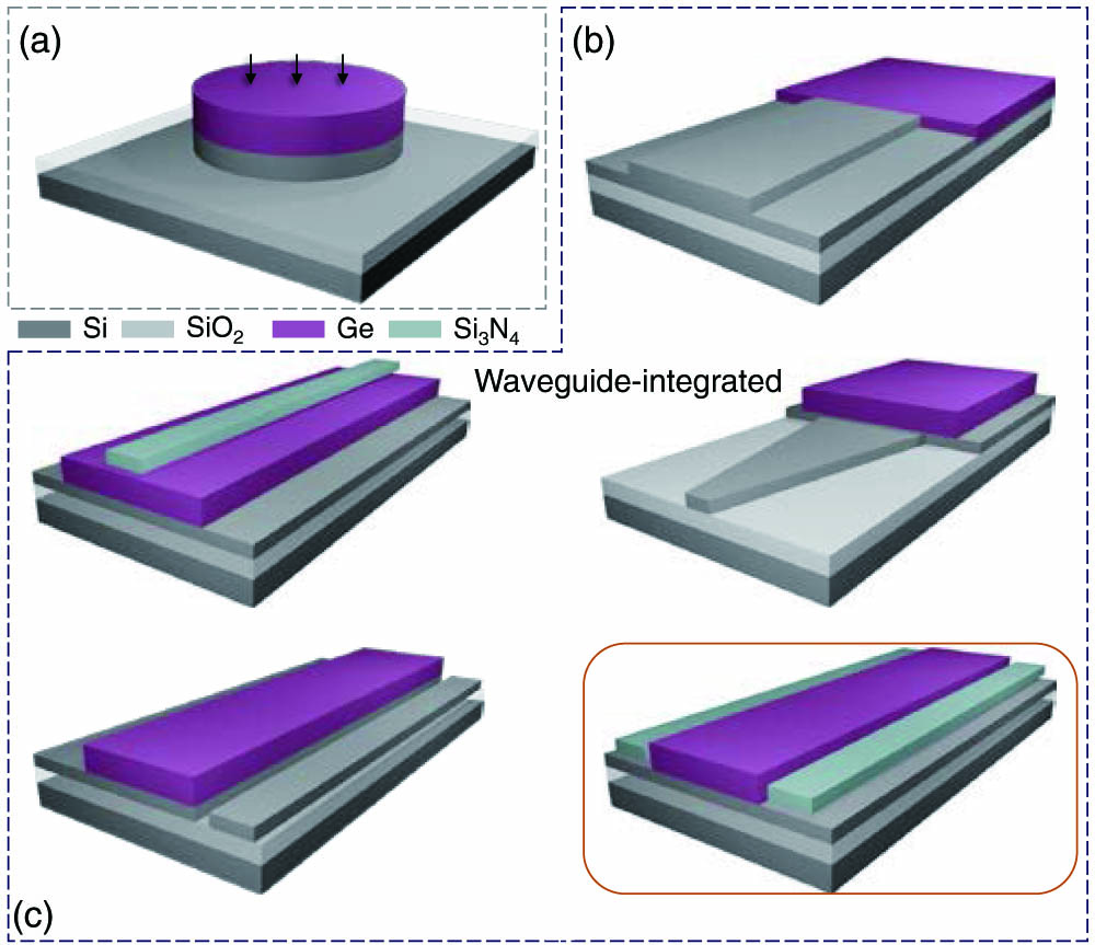
    Figure 1.Three optical coupling schemes of Ge-on-Si PD: (a) vertical incidence and waveguide-integrated coupling including (b) butt coupling and (c) evanescent coupling. In evanescent coupling the optical input waveguide can be positioned on top, at the bottom, or lateral to the absorber (germanium). The inside of the orange rectangle is the evanescent-coupling configuration based on double lateral Si3N4 waveguides, which is first proposed and demonstrated in this work.

    Compared to a Si waveguide, the Si3N4 waveguide features a large band gap and absence of two-photon or free-carrier absorption in the telecom band, ultralow propagation loss (<1  dB/m), as well as low nonlinearity and a wide-band transparency window (0.4–4.5 μm) [3538]. Additionally, several major foundries, such as AIM Photonics, CompoundTek, ST Microelectronics, and CEA-Leti, have pronounced their silicon photonic platforms integrated with at least one Si3N4 layer. However, the combining of Ge-on-Si PD with Si3N4 waveguides has not been explored much. Especially, to the best of the authors’ knowledge, a Ge-on-Si PD with a double lateral coupling scheme has not been proposed and demonstrated.

    In this paper, we report the first concept of a Ge-on-Si PD with double lateral Si3N4 waveguides, which can serve as a novel waveguide-integrated coupling configuration as shown in Fig. 1. The double lateral coupling Si3N4 waveguides will decouple the light propagation from the Ge absorption and Si slab waveguide. They allow for independent optimization of quantum efficiency, operation speed, and power handling. The Ge-on-Si PD based on lateral coupling Si3N4 waveguides has several distinctive advantages. (1) The lateral Si3N4 waveguides can be designed relatively free. This might be very beneficial to manipulating the optical field in the Ge absorption region to attain uniform photocarrier distribution, which will be helpful to improve quantum efficiency and operation speed. (2) The light propagation in the double lateral Si3N4 waveguides will avoid the optical loss caused by bottom doped silicon slab waveguide. The doping density of the silicon slab waveguide can be appropriately adjusted to achieve higher operation speed again. (3) As the χ(3) of Si3N4 is about 20 times lower than that of Si in the telecommunication wavelength range, the light propagation in the double lateral Si3N4 waveguides possesses lower nonlinearity [35]. Therefore, the Si3N4 waveguide can sustain higher optical power density than the Si waveguide and evade two-photon absorption, which means wide-input-power dynamic range. (4) The combination of high-speed Ge-on-Si PD with a Si3N4 waveguide could be a novel active Si3N4 platform that could achieve the integration of coherent receivers at 1 μm and the visible light band.

    We design and fabricate the Ge-on-Si PD with double lateral coupling Si3N4 waveguides based on a commercial standard silicon-on-insulator (SOI) platform. To comprehensively characterize the proposed lateral coupling Ge-on-Si PD, first, the static current-voltage (I-V) characteristic and responsivity are measured. Then equivalent circuit model and theoretical 3 dB OE bandwidth investigation are implemented. Second, the small-signal (S21, S11) radio-frequency (RF) measurements for the Si3N4-based lateral coupling PD are executed. Finally, the high-speed and high-power large-signal measurements, including non-return-to-zero (NRZ) on-off-keying (OOK) and four-level pulse amplitude modulation (PAM-4) eye diagrams are attained.

    2. STRUCTURE AND PRINCIPLE

    (a) Three-dimensional (3D) schematic of Ge-on-Si PD with double lateral Si3N4 waveguides. (b) Top view of Ge-on-Si PD with double lateral Si3N4 waveguides. (c) Cross-sectional view of Ge-on-Si PD with double lateral Si3N4 waveguides. (d) Cross-sectional view of the Si3N4 waveguide optical field with 800 nm and 450 nm width and the side view of the optical field distribution of the Ge absorption region. The light propagates along the x axis.

    Figure 2.(a) Three-dimensional (3D) schematic of Ge-on-Si PD with double lateral Si3N4 waveguides. (b) Top view of Ge-on-Si PD with double lateral Si3N4 waveguides. (c) Cross-sectional view of Ge-on-Si PD with double lateral Si3N4 waveguides. (d) Cross-sectional view of the Si3N4 waveguide optical field with 800 nm and 450 nm width and the side view of the optical field distribution of the Ge absorption region. The light propagates along the x axis.

    For regular butt-coupling and evanescent-coupling (bottom) schemes, the light is injected into Ge region all at once with nonuniform optical field distribution in the absorber, which will cause a large electron–hole pair density at the Ge-Si waveguide interface [13,25]. The high density of photogenerated electron–hole pairs generates relatively strong gradient of charge, which will induce a large electric field opposing to the applied external voltage. This phenomenon is called carrier screening [39,40], which will drastically degrade the 3 dB OE bandwidth. Therefore, the uniform optical field distribution in the Ge region will be helpful to generate homogeneous electron–hole pair density, and consequently, it is beneficial to improving the operation speed. Figure 2(d) shows the cross-sectional view of field distribution of the Si3N4 waveguide with 800 nm and 450 nm width and the side view of field distribution of the Ge absorption region. The light propagates along the x axis. Compared with butt coupling and evanescent coupling (bottom), it is obvious that the light spreads more uniformly in the whole Ge absorption region by using double lateral Si3N4 waveguides.

    3. EXPERIMENTAL RESULTS

    A. Optical Micrograph and Setups

    (a) Micrograph of the fabricated Ge-on-Si PD with double lateral Si3N4 waveguides. (b) and (c) Schematic of the experimental setup for the measurement of the 3 dB OE bandwidth and eye diagrams. The black and red lines represent the optical and electrical connections, respectively. PD, photodetector; AWG, arbitrary waveform generator; EDFA, erbium-doped fiber amplifier; VOA, variable optical attenuator; WSS, wavelength-selective switch; PC, polarization controller; LN MZM, lithium niobite Mach–Zehnder modulator.

    Figure 3.(a) Micrograph of the fabricated Ge-on-Si PD with double lateral Si3N4 waveguides. (b) and (c) Schematic of the experimental setup for the measurement of the 3 dB OE bandwidth and eye diagrams. The black and red lines represent the optical and electrical connections, respectively. PD, photodetector; AWG, arbitrary waveform generator; EDFA, erbium-doped fiber amplifier; VOA, variable optical attenuator; WSS, wavelength-selective switch; PC, polarization controller; LN MZM, lithium niobite Mach–Zehnder modulator.

    B. Static Measurements

    (a) Current-voltage (I-V) characteristics of Ge-on-Si PD with double lateral Si3N4 waveguides in the dark illuminated state. (b) Measured photocurrent and responsivity as a function of input optical power at −1 V bias voltage.

    Figure 4.(a) Current-voltage (I-V) characteristics of Ge-on-Si PD with double lateral Si3N4 waveguides in the dark illuminated state. (b) Measured photocurrent and responsivity as a function of input optical power at 1  V bias voltage.

    C. Equivalent Circuit Model

    (a) and (b) Experimental and fitted magnitude/phase part of the small-signal S11 reflection parameters from 100 MHz to 60 GHz at −3 V bias voltage. The inset plots the extracted equivalent circuit model of our proposed Ge-on-Si PD with lateral Si3N4 waveguides.

    Figure 5.(a) and (b) Experimental and fitted magnitude/phase part of the small-signal S11 reflection parameters from 100 MHz to 60 GHz at 3  V bias voltage. The inset plots the extracted equivalent circuit model of our proposed Ge-on-Si PD with lateral Si3N4 waveguides.

    D. Theoretical 3 dB OE Bandwidth

    To profoundly analyze the high-frequency response of the fabricated Ge-on-Si PD with double lateral Si3N4 waveguides, first, the theoretical calculation of the 3 dB OE bandwidth is presented. Then the small-signal measurements for the Ge-on-Si PD are implemented. It is well known that the RF response of a Ge-on-Si PD is largely controlled by carrier transit-time-limited bandwidth (ftr) and resistor-capacitor (RC)-limited bandwidth (fRC) in the active PIN regions [27,41]. The carrier transit frequency ftr can be written as ftr=0.45υbd,where υb is the carrier saturation drift velocity (Ge: υb=6×10⁶  cm/s) and d is the thickness of the intrinsic Ge zone. For the proposed Ge-on-Si PD with double lateral Si3N4 waveguides, the intrinsic Ge (i-Ge) region is about 0.3 μm. Therefore, the theoretical ftr is estimated to be 90 GHz. The limit of the RC bandwidth can be calculated by [27,41] fRC=12πRC,where R is the total resistance, which includes the series resistance Rs and the load resistance Rload, and C is the capacitance, including the junction capacitance Cj and the parasitic capacitance Cp. Based on the extracted parameters (R and C) from the S11 measurement, the fRC is evaluated to be approximately 82.4 GHz.

    The total 3 dB frequency response, determined by ftr and fRC, can be calculated by [41,42] f3dB=1fRC2+ftr2.Therefore, the theoretical 3 dB OE bandwidth f3dB of a Ge-on-Si PD with lateral Si3N4 waveguides is evaluated to be approximately 60.8 GHz.

    E. Small-Signal Measurements

    (a) Normalized RF response of the Ge-on-Si PD with lateral Si3N4 waveguides. The bias voltage is fixed at −3 V. (b) Measured 3 dB OE bandwidths with different photocurrent levels. The inset plots the experimental and fitted results of the S21 transmission parameter under 4 mA photocurrent.

    Figure 6.(a) Normalized RF response of the Ge-on-Si PD with lateral Si3N4 waveguides. The bias voltage is fixed at 3  V. (b) Measured 3 dB OE bandwidths with different photocurrent levels. The inset plots the experimental and fitted results of the S21 transmission parameter under 4 mA photocurrent.

    F. Large-Signal Eye Diagram Measurements

    Measured 70, 80, 90, and 100 Gbit/s NRZ eye diagrams under 3 V reverse-bias voltage.

    Figure 7.Measured 70, 80, 90, and 100 Gbit/s NRZ eye diagrams under 3 V reverse-bias voltage.

    Measured 100, 120, 140, and 150 Gbit/s PAM-4 eye diagrams under 3 V reverse-bias voltage.

    Figure 8.Measured 100, 120, 140, and 150 Gbit/s PAM-4 eye diagrams under 3 V reverse-bias voltage.

    Measured 60 Gbit/s NRZ eye diagrams with 5, 10, 15, and 20 mA photocurrent at the DC bias voltage of −3 V.

    Figure 9.Measured 60 Gbit/s NRZ eye diagrams with 5, 10, 15, and 20 mA photocurrent at the DC bias voltage of 3  V.

    4. DISCUSSION

    Compared to the butt-coupling scheme, the possible freely chosen parameters of an evanescent-coupling configuration based on double lateral Si3N4 waveguides include waveguide thickness, gap width, and waveguide shape (strip or rib or tapered waveguide and so on). One difference between the coupling configuration of the Si3N4 waveguide on top and on the double lateral sides of the absorber is the way to adjust the gap width between the Si3N4 and the absorber. For the Si3N4 waveguide on top of the absorber, in order to change the gap width, the thickness of the silica (SiO2) layer has to be adjusted during the fabrication processes. Nevertheless, for the Si3N4 waveguide on the double lateral sides of the absorber, the variation of gap width can be realized just by designing the layout. It is very easy and accessible. Another difference is the light evanescent coupling from one side and both sides. For high input optical power, it is well known that the capability to manipulate the optical field in the absorption region to attain uniform photocarrier distribution is very beneficial to improving quantum efficiency and operation speed [34,39,42,43]. The evanescent coupling from both sides has the advantage of manipulating the optical field in the absorber. Although the lateral Si3N4 waveguides can be designed relatively free, in order to achieve high coupling efficiency, there are still trade-offs between Ge absorber thickness, gap width, and Si3N4 waveguide thickness [33].

    In our proposed structure, the silicon-based 1×2 MMI splitter and the two Si to Si3N4 inter-layer transitions are integral parts of the proposed Ge-on-Si PD. The losses of the silicon-based 1×2 MMI splitter and Si to Si3N4 inter-layer transition are about 0.3 dB and 0.2 dB, respectively. The responsivity of the Ge-on-Si PD is about 0.36 A/W without correcting for the losses of these components (0.5 dB). In future designed structures, the silicon-based 1×2 MMI splitter and Si to Si3N4 inter-layer transitions can be replaced by a Si3N4-based 1×2 MMI splitter, which might further decrease the losses and improve the internal responsivity. The evanescent coupling from both sides will lead to a standing wave pattern in the absorber as shown in Fig. 2(d). This phenomenon is similar to the Ge-on-Si PD with four-directional light input [42], but its effect on optical signal reception can be nearly ignored.

    5. CONCLUSION

    In summary, as a proof-of-concept demonstration, we have proposed a novel light coupling scheme of waveguide-integrated Ge-on-Si PD: lateral coupling by employing double lateral Si3N4 waveguides. It features uniform optical field distribution in the Ge absorption region and allows for independent optimization of quantum efficiency, operation speed, and power handling. The maximum responsivity is estimated to be approximately 0.52 A/W with 25 mW input power at 1550 nm, which can be further enhanced by decreasing the gap between the Si3N4 waveguide and the 220 nm Si slab and increasing the gap between the Si3N4 waveguide and the metal copper. Based on the equivalent circuit model and extracted parameters, the Ge-on-Si PDs with double lateral Si3N4 waveguides have reached theoretical 3 dB OE bandwidths of up to 60.8 GHz, which is well matched to the experimentally demonstrated 60 GHz under 4 mA photocurrent at DC bias voltage 3  V. Under 1 mA photocurrent, the 70, 80, 90, and 100 Gbit/s NRZ and 100, 120, 140, and 150 Gbit/s PAM-4 clear openings of the eye diagrams are obtained without utilizing any offline DSP at the RX side. The clear open electrical eye diagrams of 60 Gbit/s NRZ under 5, 10, 15, and 20 mA photocurrent at the DC bias voltage of 3  V are also attained, which exhibits the detection capability of high-speed and high-power signal. We are currently making great efforts to improve the quantum efficiency and further explore the high-speed and high-power handling ability of Ge-on-Si PD with double lateral Si3N4 waveguides. Overall, the proposed lateral Si3N4 waveguide structure is flexibly extendable to the light coupling scheme, which shows favorable performances. It is believed that our proposed Ge-on-Si PD has the great potential to achieve low-complexity and low-cost >100  Gbit/s data reception per lane for future 400/800 GbE transceivers, which can be utilized in data centers, long-haul telecommunication, and high-performance computers. The characteristic of high-speed and wide-input-power dynamic range makes it attractive to integrated microwave photonics application, such as ultra-broadband wireless communication.

    References

    [1] R. A. Soref. Silicon-based optoelectronics. Proc. IEEE, 81, 1687-1706(1993).

    [2] D. A. B. Miller. Device requirements for optical interconnects to silicon chips. Proc. IEEE, 97, 1166-1185(2009).

    [3] M. Asghari, A. V. Krishnamoorthy. Energy-efficient communication. Nat. Photonics, 5, 268-270(2011).

    [4] D. Thomson, A. Zilkie, J. E. Bowers, T. Komljenovic, G. T. Reed, L. Vivien, D. Marris-Morini, E. Cassan, L. Virot, J. M. Fédéli, J.-M. Hartmann, J. H. Schmid, D. X. Xu, F. Boeuf, P. O’Brien, G. Z. Mashanovich, M. Nedeljkovic. Roadmap on silicon photonics. J. Opt., 18, 073003(2016).

    [5] K. Yamada, T. Tsuchizawa, H. Nishi, R. Kou, T. Hiraki, K. Takeda, H. Fukuda, Y. Ishikawa, K. Wada, T. Yamamoto. High-performance silicon photonics technology for telecommunications applications. Sci. Technol. Adv. Mater., 15, 024603(2014).

    [6] G. Zhang, J. Y. Haw, H. Cai, F. Xu, S. M. Assad, J. F. Fitzsimons, X. Zhou, Y. Zhang, S. Yu, J. Wu, W. Ser, L. C. Kwek, A. Q. Liu. An integrated silicon photonic chip platform for continuous-variable quantum key distribution. Nat. Photonics, 13, 839-842(2019).

    [7] Y. Shen, N. Harris, S. Skirlo, M. Prabhu, T. Baehr-Jones, M. Hochberg, X. Sun, S. Zhao, H. Larochelle, D. Englund, M. Soljačić. Deep learning with coherent nanophotonic circuits. Nat. Photonics, 11, 441-446(2017).

    [8] D. Marpaung, J. Yao, J. Capmany. Integrated microwave photonics. Nat. Photonics, 13, 80-90(2019).

    [9] D. Marris-Morini, V. Vakarin, J. M. Ramirez, Q. Liu, A. Ballabio, J. Frigerio, M. Montesinos, C. Alonso-Ramos, X. Le Roux, S. Serna, D. Benedikovic, D. Chrastina, L. Vivien, G. Isella. Germanium based integrated photonics from near- to mid-infrared applications. Nanophotonics, 7, 1781-1793(2018).

    [10] J. Michel, J. Liu, L. C. Kimerling. High-performance Ge-on-Si photodetectors. Nat. Photonics, 4, 527-534(2010).

    [11] Y. Ishikawa, K. Wada, D. D. Cannan, J. Liu, D. L. Hsin-Chiao, L. C. Kimerling. Strain-induced band gap shrinkage in Ge grown on Si substrate. Appl. Phys. Lett., 82, 2044-2046(2003).

    [12] J. F. Liu, J. Michel, W. Giziewicz, D. Pan, K. Wada, D. Cannon, L. C. Kimerling, J. Chen, F. O. Ilday, F. X. Kartner, J. Yasaitis. High-performance, tensile strained Ge p-i-n photodetectors on a Si platform. Appl. Phys. Lett., 87, 103501(2005).

    [13] R. Anthony, D. E. Hagan, D. Genuth-Okon, L. M. Maestro, I. F. Crowe, M. P. Halsall, A. P. Knights. Extended wavelength responsivity of a germanium photodetector integrated with a silicon waveguide exploiting the indirect transition. IEEE J. Sel. Top. Quantum Electron., 26, 3800107(2020).

    [14] H. Chen, M. Galili, P. Verheyen, P. De Heyn, G. Lepage, J. De Coster, S. Balakrishnan, P. Absil, L. Oxenlowe, J. Van Campenhout, G. Roelken. 100-Gbps RZ data reception in 67-GHz Si-contacted germanium waveguide p-i-n photodetectors. J. Lightwave Technol., 35, 722-726(2017).

    [15] M. Rouviere, M. Halbwax, J.-L. Cercus, E. Cassan, L. Vivien, D. Pascal, M. Heitzmann, J.-M. Hartmann, S. Laval. Integration of germanium waveguide photodetectors for intrachip optical interconnects. Opt. Eng., 44, 75402-75406(2005).

    [16] D. Dai, M. Piels, J. E. Bowers. Monolithic germanium/silicon photodetectors with decoupled structures: resonant APDs and UTC photodiodes. IEEE J. Sel. Top. Quantum Electron., 20, 3802214(2014).

    [17] L. Colace, G. Masini, F. Galluzzi, G. Assanto, G. Capellini, L. Di Gaspare, E. Palange, F. Evangelisti. Metal-semiconductor-metal near-infrared light detector based on epitaxial Ge/Si. Appl. Phys. Lett., 72, 3175-3177(1998).

    [18] H. C. Luan, D. R. Lim, K. K. Lee, K. M. Chen, L. C. Kimerling. High-quality Ge epilayers on Si with low threading-dislocation densities. Appl. Phys. Lett., 75, 2909-2911(1999).

    [19] M. Halbwax, D. Bouchier, V. Yam, D. Debarre, L. H. Nguyen, Y. Zheng, P. Rosner, M. Benamara, H. P. Strunk, C. Clerc. Kinetics of Ge growth at low temperature on Si (001) by ultrahigh vacuum chemical vapor deposition. J. Appl. Phys., 97, 064907(2005).

    [20] J. Liu, R. Camacho-Aguilera, J. T. Bessette, X. Sun, X. Wang, Y. Cai, L. C. Kimerling, J. Michel. Ge-on-Si optoelectronics. Thin Solid Films, 520, 3354-3360(2012).

    [21] L. Chen, P. Dong, M. Lipson. High performance germanium photodetectors integrated on submicron silicon waveguides by low temperature wafer bonding. Opt. Express, 16, 11513-11518(2008).

    [22] Z. Huang, J. Oh, J. C. Campbell. Back-side-illuminated high-speed Ge photodetector fabricated on Si substrate using thin SiGe buffer layers. Appl. Phys. Lett., 85, 3286-3288(2004).

    [23] D. Ahn, C. Hong, J. Liu, W. Giziewicz, M. Beals, L. C. Kimerling, J. Michel. High performance, waveguide integrated Ge photodetectors. Opt. Express, 15, 3916-3921(2007).

    [24] X. Li, L. Peng, Z. Liu, X. Liu, J. Zheng, Y. Zuo, C. Xue, B. Cheng. High-power back-to-back dual-absorption germanium photodetector. Opt. Lett., 45, 1358-1361(2020).

    [25] H. Chen, P. Verheyen, P. De Heyn, G. Lepage, J. De Coster, P. Absil, G. Roelkens, J. Van Campenhout. High-responsivity low-voltage 28-Gb/s Ge p-i-n photodetector with silicon contacts. J. Lightwave Technol., 33, 820-824(2015).

    [26] H. Chen, P. Verheyen, P. De Heyn, G. Lepage, J. De Coster, S. Balakrishnan, P. Absil, W. Yao, L. Shen, G. Roelkens, J. Van Campenhou. −1 V bias 67 GHz bandwidth Si-contacted germanium waveguide p-i-n photodetector for optical links at 56 Gbps and beyond. Opt. Express, 24, 4622-4631(2016).

    [27] Z. Liu, F. Yang, W. Wu, H. Cong, J. Zheng, C. Li, C. Xue, B. Cheng, Q. Wang. 48 GHz high-performance Ge-on-SOI photodetector with zero-bias 40 Gbps grown by selective epitaxial growth. J. Lightwave Technol., 35, 5306-5310(2017).

    [28] D. Benedikovic, L. Virot, G. Aubin, F. Amar, B. Szelag, B. Karakus, J. M. Hartmann, C. Alonso-Ramos, X. L. Roux, P. Crozat, E. Cassan, D. Marris-Morini, C. Baudot, F. Boeuf, J. M. Fédéli, C. Kopp, L. Vivien. 25 Gbps low-voltage hetero-structured silicon-germanium waveguide pin photodetectors for monolithic on-chip nanophotonic architectures. Photon. Res., 7, 437-444(2019).

    [29] D. Benedikovic, L. Virot, G. Aubin, J. M. Hartmann, F. Amar, B. Szelag, X. L. Roux, C. Alonso-Ramos, P. Crozat, É. Cassan, D. Marris-Morini, C. Baudot, F. Boeuf, J. M. Fédéli, C. Kopp, L. Vivien. Comprehensive study on chip-integrated germanium PIN photodetectors for energy-efficient silicon interconnects. IEEE J. Sel. Top. Quantum Electron., 56, 8400409(2020).

    [30] L. Vivien, M. Rouvière, J. M. Fédéli, D. Marris-Morini, J. F. Damlencourt, J. Mangeney, P. Crozat, L. E. Melhaoui, E. Cassan, X. L. Roux, D. Pascal, S. Laval. High speed and high responsivity germanium photodetector integrated in a silicon-on-insulator microwaveguide. Opt. Express, 15, 9843-9848(2007).

    [31] C. T. DeRose, D. C. Trotter, W. A. Zortman, A. L. Starbuck, M. Fisher, M. R. Watts, P. S. Davids. Ultra compact 45 GHz CMOS compatible germanium waveguide photodiode with low dark current. Opt. Express, 19, 24897-24904(2011).

    [32] J. Cui, Z. Zhou. High-performance Ge-on-Si photodetector with optimized DBR location. Opt. Lett., 42, 5141-5144(2017).

    [33] D. Ahn, L. C. Kimerling, J. Michel. Efficient evanescent wave coupling conditions for waveguide-integrated thin-film Si/Ge photodetectors on silicon-on-insulator/germanium-on-insulator substrates. J. Appl. Phys., 110, 083115(2011).

    [34] M. J. Byrd, E. Timurdogan, Z. Su, C. V. Poulton, M. R. Watts. Mode-evolution-based coupler for high saturation power Ge-on-Si photodetectors. Opt. Lett., 42, 851-854(2017).

    [35] C. H. Henry, R. F. Kazarinov, H. J. Lee, K. J. Orlowsky, L. E. Katz. Low loss Si3N4-SiO2 optical waveguides on Si. Appl. Opt., 26, 2621-2624(1987).

    [36] P. Muñoz, G. Micó, L. A. Bru, D. Pastor, D. Pérez, J. D. Doménech, J. Fernández, R. Baños, B. Gargallo, R. Alemany, A. M. Sánchez, J. M. Cirera, R. Mas, C. Domínguez. Silicon nitride photonic integration platforms for visible, near-infrared and mid-infrared applications. Sensors, 17, 2088(2017).

    [37] C. G. H. Roeloffzen, M. Hoekman, E. J. Klein, L. S. Wevers, R. B. Timens, D. Marchenko, D. Geskus, R. Dekker, A. Alippi, R. Grootjans, A. V. Rees, R. M. Oldenbeuving, J. P. Epping, R. G. Heideman, K. Worhoff, A. Leinse, D. Geuzebroek, E. Schreuder, P. W. L. van Dijk, I. Visscher, C. Taddei, Y. Fan, C. Taballione, Y. Liu, D. Marpaung, L. Zhuang, M. Benelajla, K. J. Boller. Low-loss Si3N4 TriPleX optical waveguides: technology and applications overview. IEEE J. Sel. Top. Quantum Electron., 24, 4400321(2018).

    [38] D. J. Blumenthal, R. Heideman, D. Geuzebroek, A. Leinse, C. Roeloffzen. Silicon nitride in silicon photonics. Proc. IEEE, 106, 2209-2231(2018).

    [39] K. S. Giboney, M. J. W. Rodwell, J. E. Bowers. Travelling-wave photodetector design and measurements. IEEE J. Sel. Top. Quantum Electron., 2, 622-629(1996).

    [40] A. Beling, X. Xie, J. C. Campbell. High-power, high-linearity photodiodes. Optica, 3, 328-338(2016).

    [41] M. Oehme, J. Werner, E. Kasper, M. Jutzi, M. Berroth. High bandwidth Ge p-i-n photodetector integrated on Si. Appl. Phys. Lett., 89, 071117(2006).

    [42] X. Hu, D. Wu, H. Zhang, W. Li, D. Chen, L. Wang, X. Xiao, S. Yu. High-speed lateral PIN germanium photodetector with 4-directional light input. Opt. Express, 28, 38343-38354(2020).

    [43] Y. Zuo, Y. Yu, Y. Zhang, D. Zhou, X. L. Zhang. Integrated high-power germanium photodetectors assisted by light field manipulation. Opt. Lett., 44, 3338-3341(2019).

    Xiao Hu, Dingyi Wu, Hongguang Zhang, Weizhong Li, Daigao Chen, Lei Wang, Xi Xiao, Shaohua Yu. High-speed and high-power germanium photodetector with a lateral silicon nitride waveguide[J]. Photonics Research, 2021, 9(5): 749
    Download Citation