• Chinese Optics Letters
  • Vol. 17, Issue 3, 031403 (2019)
Chong Shan1, Yuanan Zhao2、3、*, Yanqi Gao1、4, Xiaohui Zhao1, Guohang Hu2, Weixin Ma1, and Jianda Shao2、**
Author Affiliations
  • 1Shanghai Institute of Laser Plasma, China Academy of Engineering Physics, Shanghai 201800, China
  • 2Key Laboratory of Materials for High Power Laser, Shanghai Institute of Optics and Fine Mechanics, Chinese Academy of Sciences, Shanghai 201800, China
  • 3State Key Laboratory of Applied Optics, Changchun Institute of Optics, Fine Mechanics and Physics, Chinese Academy of Sciences, Changchun 130033, China
  • 4IFSA Collaborative Innovation Center, Shanghai Jiao Tong University, Shanghai 200240, China
  • show less
    DOI: 10.3788/COL201917.031403 Cite this Article Set citation alerts
    Chong Shan, Yuanan Zhao, Yanqi Gao, Xiaohui Zhao, Guohang Hu, Weixin Ma, Jianda Shao. Laser-induced defects in optical multilayer coatings by the spatial resolved method[J]. Chinese Optics Letters, 2019, 17(3): 031403 Copy Citation Text show less
    Schematic diagram of spatial resolved damage testing system.
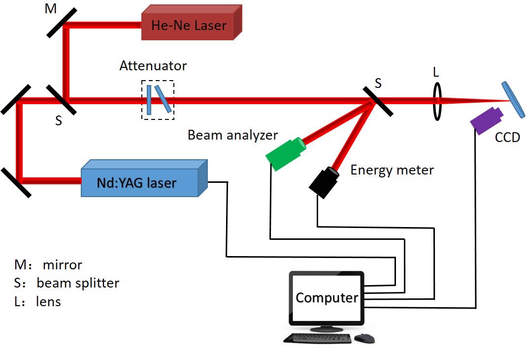
    Fig. 1. Schematic diagram of spatial resolved damage testing system.
    Nd:YAG laser beam position at the wavelength of 355 nm with 0.5 J/cm2 laser peak fluence in (a) the beam profiler and (b) the CCD camera. The silver film was tested for beam position calibration.
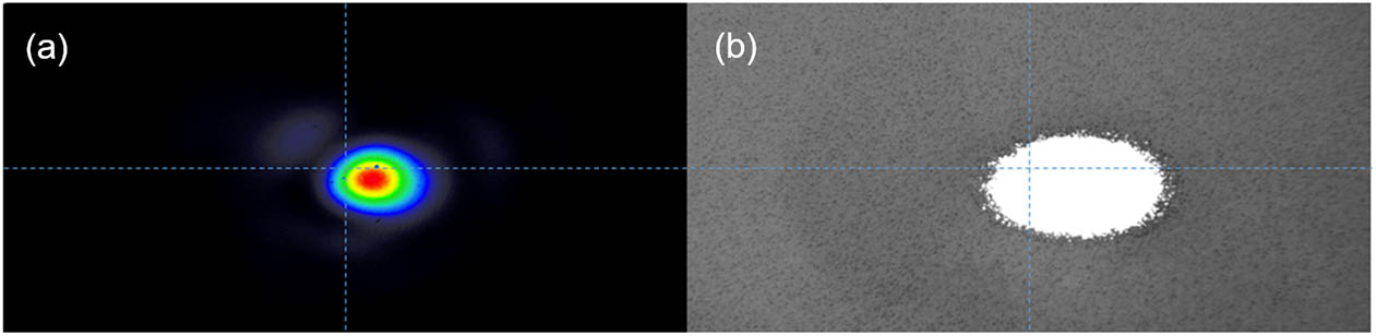
    Fig. 2. Nd:YAG laser beam position at the wavelength of 355 nm with 0.5J/cm2 laser peak fluence in (a) the beam profiler and (b) the CCD camera. The silver film was tested for beam position calibration.
    (a) Recorded picture of the sample before laser irradiation. (b) Defect damage position in the Gaussian beam after laser irradiation at the wavelength of 355 nm with 26.4 J/cm2 peak fluence. The triple frequency splitter was tested for the defect damage threshold. The elliptical shadow with rings around it in the middle of the image is illumination light for observing the defect damage position in the CCD camera.
    Fig. 3. (a) Recorded picture of the sample before laser irradiation. (b) Defect damage position in the Gaussian beam after laser irradiation at the wavelength of 355 nm with 26.4J/cm2 peak fluence. The triple frequency splitter was tested for the defect damage threshold. The elliptical shadow with rings around it in the middle of the image is illumination light for observing the defect damage position in the CCD camera.
    Transmittance spectrum of the multilayer coating prepared via reactive e-beam evaporation.
    Fig. 4. Transmittance spectrum of the multilayer coating prepared via reactive e-beam evaporation.
    SEM images of defect damages: class A was irradiated by the 355 nm laser with fluence of (a) 5.69 J/cm2 and (b) 7.16 J/cm2, respectively; class B was irradiated by the 355 nm laser with the fluence of (c) 8.33 J/cm2 and (d) 7.62 J/cm2, respectively.
    Fig. 5. SEM images of defect damages: class A was irradiated by the 355 nm laser with fluence of (a) 5.69J/cm2 and (b) 7.16J/cm2, respectively; class B was irradiated by the 355 nm laser with the fluence of (c) 8.33J/cm2 and (d) 7.62J/cm2, respectively.
    Electric field of the triple frequency splitter by the 355 nm laser.
    Fig. 6. Electric field of the triple frequency splitter by the 355 nm laser.
    (a), (b) SEM images and (c),(d) FIB images: class B defect damage morphology of the triple frequency splitter by the 355 nm laser irradiation with the fluence of (a) 9.15 J/cm2 and (b) 6.81 J/cm2, respectively; (c) and (d) recorded depth information of class B defect damage morphology.
    Fig. 7. (a), (b) SEM images and (c),(d) FIB images: class B defect damage morphology of the triple frequency splitter by the 355 nm laser irradiation with the fluence of (a) 9.15J/cm2 and (b) 6.81J/cm2, respectively; (c) and (d) recorded depth information of class B defect damage morphology.
    SEM images of defect damages: class A was irradiated by the 532 nm laser with the fluence of (a) 5.26 J/cm2 and (b) 7.12 J/cm2, respectively; class B was irradiated by the 355 nm laser with the fluence of (c) 8.93 J/cm2 and (d) 13.66 J/cm2, respectively.
    Fig. 8. SEM images of defect damages: class A was irradiated by the 532 nm laser with the fluence of (a) 5.26J/cm2 and (b) 7.12J/cm2, respectively; class B was irradiated by the 355 nm laser with the fluence of (c) 8.93J/cm2 and (d) 13.66J/cm2, respectively.
    Electric field of the triple frequency splitter irradiated by the 532 nm laser.
    Fig. 9. Electric field of the triple frequency splitter irradiated by the 532 nm laser.
    Class1-on-1 Method (J/cm2)Spatial Resolved Method (J/cm2)
    Class A9.611.63
    Class B15.734.38
    Table 1. Results of the Defect Damage Threshold of the Triple Frequency Splitter by Only the 355 nm Laser
    Class1-on-1 Method (J/cm2)Spatial Resolved Method (J/cm2)
    Class C14.175.26
    Class D19.368.33
    Table 2. Result of the Defect Damage Threshold of the Triple Frequency Splitter by Only the 532 nm Laser
    Chong Shan, Yuanan Zhao, Yanqi Gao, Xiaohui Zhao, Guohang Hu, Weixin Ma, Jianda Shao. Laser-induced defects in optical multilayer coatings by the spatial resolved method[J]. Chinese Optics Letters, 2019, 17(3): 031403
    Download Citation