1Shanghai Institute of Laser Plasma, China Academy of Engineering Physics, Shanghai 201800, China
2Key Laboratory of Materials for High Power Laser, Shanghai Institute of Optics and Fine Mechanics, Chinese Academy of Sciences, Shanghai 201800, China
3State Key Laboratory of Applied Optics, Changchun Institute of Optics, Fine Mechanics and Physics, Chinese Academy of Sciences, Changchun 130033, China
4IFSA Collaborative Innovation Center, Shanghai Jiao Tong University, Shanghai 200240, China
The spatial resolved method, which measures the laser-induced damage fluence by identifying the location of the damage point in the Gaussian beam three-dimensional direction, is demonstrated. The advantages and practicality of this method have been explained. Taking a triple frequency beam splitter as an example, the defect damage fluence can be accurately calculated by the spatial resolved method. The different defect damage performance of the triple frequency splitter is distinguished under irradiations of only the 355 and 532 nm lasers. The spatial resolved method provides a way to obtain precise information of optical film defect information.
There is a wide range of applications of the optical film in the high-power laser-driven inertial confinement fusion (ICF) and other large optical systems[1–6]. However, the laser damage issue of optical films has always been the bottleneck technology that restricts its development. The defect of optical film is the main source of damages in long pulse laser irradiation[7–15]. The laser-induced damage threshold of the defect can be more than ten times smaller than that associated with the intrinsic material[16]. Therefore, the accurate defect information is an important part of studying the laser damage mechanism of optical films. A number of pioneering studies have been conducted by some research groups on defects information[17–22].
The preliminary study of defect information set the uneven distribution of defect damage and the laser energy as an even distribution in the Gaussian beam. The defect laser damage fluence was recorded as the peak laser fluence. In the practical laser damage test, there are many kinds of defects causing laser damage in the optical film, and the laser fluence of each defect inducing damage is also different; these kinds of defects are distributed randomly in the horizontal () and vertical () directions of the optical film. The temporal and spatial energy distribution is uneven in the Gaussian laser beam. Some researches about defect damage threshold through temporal information have been reported[23,24]. However, the distribution of the electric field at the optical film is modulated by the film structure in the direction, and the effect of the electric field on the defect damage threshold has not been researched before. Therefore, combining the subdivision of the spatially resolved energy distribution with the normalization of the optical film electric field distribution is a more accurate method to analyze the defects information in the optical film.
In this Letter, the effects of laser energy distribution and electric field distribution on defects information analysis were considered. The spatial resolved test method was used to research and classify the defects information of the triple frequency splitters irradiated by the laser with wavelengths of only 355 and 532 nm.
Sign up for Chinese Optics Letters TOC. Get the latest issue of Chinese Optics Letters delivered right to you!Sign up now
In the traditional laser damage test method, in the Gaussian beam, the effective beam spot area () is obtained by the Gaussian beam area () divided by two. It can be written as where is the beam radius at of the Gaussian beam (beam waist). The laser peak fluence () is obtained by the ratio of the peak energy () to the effective spot area (). It is taken as the laser fluence causing the defect damage[25] and can be expressed as
However, the distribution of laser energy and the defect damage are not even in the Gaussian beam. The defect fluence () can be obtained by judging the incident peak fluence () and defect damage point position () in the direction in the Gaussian beam, where and are the position of the defect damage point in the direction in the Gaussian beam. The defect damage point depth in the direction and electric distribution also need to be identified. Finally, the defect damage fluence can be calculated by combining the laser fluence in the direction with the normalization of the electric field in the direction in the optical film.
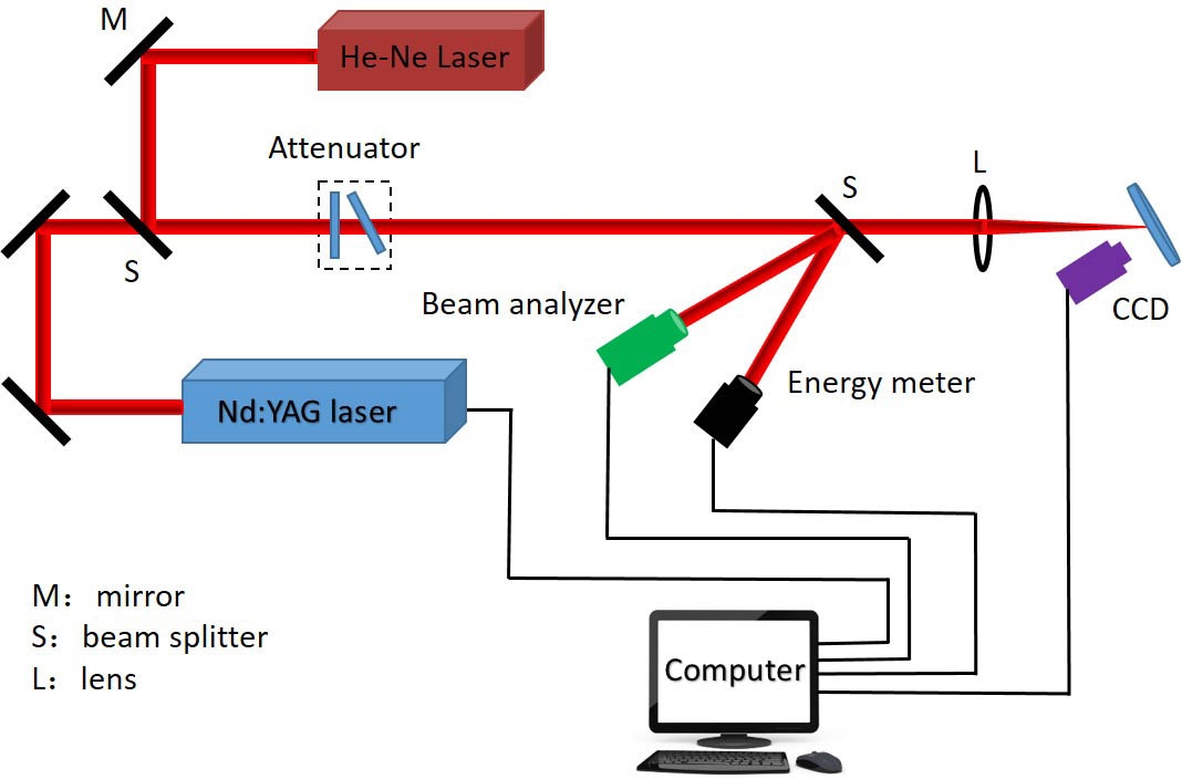
The schematic diagram of the spatial resolved test system is shown in Fig. 1. The Gaussian laser is obliquely incident on the surface of the test sample with an angle of 45° after the attenuation system, and the focal length of the lens is 5 m. The coordinate of laser damage is observed by a CCD camera with a pixel size of placed after irradiation.
Figure 1.Schematic diagram of spatial resolved damage testing system.
The core step of the spatial resolved test was to calibrate the coordinates of the defect damage points and the spatial energy in the Gaussian beam. The laser beam photograph was recorded in the laser beam analyzer (as shown in Fig. 2). At the same time, with a silver film for calibrating, and irradiated by a Nd-doped yttrium aluminum garnet (Nd:YAG) laser, the Gaussian beam position and contour on the surface were recorded by CCD. The incident peak fluence of the laser was . The laser beam information in the CCD was calibrated by comparing the beam position, contour, and special points in the two images.
Figure 2.Nd:YAG laser beam position at the wavelength of 355 nm with laser peak fluence in (a) the beam profiler and (b) the CCD camera. The silver film was tested for beam position calibration.
The test sample is irradiated for a certain number by constant laser peak fluence. In order to compare the spatial resolved method with the one-on-one test method objectively, the two test methods were set to the same laser test number, which was 100 times. That is to say, one position is irradiated with a single pulse, and then the test sample was moved to complete the experiment at 100 positions. The defect damage point position was recorded after each laser irradiation by a CCD camera. The defect damage point position is shown in Fig. 3. The defect damage laser fluence was calculated accurately according to Eq. (3) in the direction. The depth of defect damage and the corresponding electric field distribution can be observed in the direction by a scanning electron microscope (SEM) and a focused ion beam (FIB). Finally, the defect damage fluence can be obtained accurately. The distribution of energy in the temporal dimension was ignored in this Letter.
Figure 3.(a) Recorded picture of the sample before laser irradiation. (b) Defect damage position in the Gaussian beam after laser irradiation at the wavelength of 355 nm with peak fluence. The triple frequency splitter was tested for the defect damage threshold. The elliptical shadow with rings around it in the middle of the image is illumination light for observing the defect damage position in the CCD camera.
In this Letter, the triple frequency splitter was chosen as the sample, which was deposited with via electron beam evaporation, and it was designed to reflect the 355 nm laser while transmitting the 532 nm laser. The coating design was G/L0.5HL (HL)^14 H/A, where G, H, L, and A denote the substrate, layer of , layers of , and air, respectively. Figure 4 shows the transmission spectrum of the coating, which was measured by a PerkinElmer Lambda 1050 UV/VIS/NIR spectrometer at an incident angle of 45° with a wavelength range of 200–1200 nm. The transmittance for 532 nm was 92%, whereas that for 355 nm was 0.14%, as shown in Fig. 4.
Figure 4.Transmittance spectrum of the multilayer coating prepared via reactive e-beam evaporation.
The 355 nm laser irradiated the triple frequency splitter film with high reflection characteristics. The pulse width of the 355 nm laser was 6.9 ns, and the effective beam spot area was . The incident laser peak fluence of the spatial resolved method will not affect the result of the defect damage threshold measurement[26]. In order to ensure the introduction of a sufficient number of defect damages and no intrinsic damage being introduced, the incident laser peak fluence of 355 nm was set as . There were 132 defect damage points in the Gaussian beam by 100 times tests. Most of them were clustered around the center of the Gaussian beam. To obtain further information about the defect damage, including the morphologies, a detailed observation of the defect damage was performed via SEM and FIB. Figure 5 shows the defect damage morphologies at the 355 nm laser, and the defect damage morphologies can be divided into two kinds: class A and class B.
Figure 5.SEM images of defect damages: class A was irradiated by the 355 nm laser with fluence of (a) and (b) , respectively; class B was irradiated by the 355 nm laser with the fluence of (c) and (d) , respectively.
Class A defect damage was an independent circular laser damage morphology without any additional defect damage. There were 86 class A defect damages with random distribution in the Gaussian beam. Class B defect damage morphology was a circular damage accompanied by a deep crack damage. There were 46 class B defect damages distributed at the center of the Gaussian beam.
Since the peak electric field was mainly distributed on the surface of the optical film (as shown in Fig. 6), in the experiment, the defect damage irradiated by the 355 nm laser was caused by the defect absorbing amount of laser energy under the high electric field, mainly in the first eight layers of the film.
Figure 6.Electric field of the triple frequency splitter by the 355 nm laser.
The class B defect damage was caused by the defect in the first eight layers of the optical film and the scratches or pit defects existing on the surface of the substrate. Some research groups have done much work on this kind of laser damage morphology and mechanism[27,28]. The crack defect in the optical film was caused by scratches or pit defects after e-beam deposition on the surface of the substrate. According to the thermal transfer theory, a phenomenological model is proposed to describe the formation of this damage. At the beginning, the defect absorbed the laser energy under the high electric field in the first eight layers of the optical film. As a result, there was an extremely unstable and high-temperature melting point at the initial position of the defect damage, and the melting point became a new source of crack damage. The range of the damage was increased by the expanding plasma scald in the and directions. The class B defect damage was formed when the plasma penetrated into the crack defect in the direction in the optical film (as shown in Fig. 7). Therefore, the initial damage of the class B defect should be caused by the defects in the first eight layers of the optical film, and the electric field normalization was based on the initial defect damage position in the direction in the optical film.
Figure 7.(a), (b) SEM images and (c),(d) FIB images: class B defect damage morphology of the triple frequency splitter by the 355 nm laser irradiation with the fluence of (a) and (b) , respectively; (c) and (d) recorded depth information of class B defect damage morphology.
Finally, compared with the one-on-one method, we accurately calculated the defect damage threshold of two kinds of defect damages by the spatial resolved method. The test result of the defect damage threshold is shown in Table 1.
Class
1-on-1 Method (J/cm2)
Spatial Resolved Method (J/cm2)
Class A
9.61
1.63
Class B
15.73
4.38
Table 1. Results of the Defect Damage Threshold of the Triple Frequency Splitter by Only the 355 nm Laser
Then, the triple frequency splitter film was irradiated by the 532 nm laser. The incident laser peak fluence was . The pulse width of the 532 nm laser was 9.6 ns, and the effective beam spot area was . There were 119 defect damages after 100 times tests. Typical damage morphologies of the samples induced by the 532 nm laser were also obtained (Fig. 8). The defect damages occurred mainly on the substrate of the optical film. The reason was that the triple frequency splitter irradiated by the 532 nm laser showed transmittance. There was no particular peak electric field in the entire optical film (shown in Fig. 9). The defect was contributed by the processing and cleaning of the substrate in the air. Therefore, it was well understood that the defect damage occurred at the substrate in the splitter film[29,30].
Figure 8.SEM images of defect damages: class A was irradiated by the 532 nm laser with the fluence of (a) and (b) , respectively; class B was irradiated by the 355 nm laser with the fluence of (c) and (d) , respectively.
There were also two kinds of defect damage morphologies, class C and class D. The class C defect damage morphologies are shown in Figs. 8(a) and 8(b). The size of these defect damages was between 12 and 24 μm. Class C was caused by submicron defects on the surface of the substrate. There were 74 class C defect damages, and these defect damages were distributed randomly in the profile of the incident Gaussian beam.
The second kind of defect damage morphology was shown in Figs. 8(c) and 8(d). The size of the class D defect damages was between 35 and 45 μm. Class D defect damage was mainly caused by micron-scale defects existing on the surface of the substrate. There were 45 class D defect damages in our experiments. This type of defect damage was mainly distributed in the center of the Gaussian beam. Finally, the laser damage thresholds of the two kinds of defects were shown in Table 2 by the one-on-one and spatial resolved test methods. The defects break through the film stress, spraying out and causing the damage by absorbing the laser energy. Therefore, the larger the area of defect damage, the greater the film stress that needs to be broken, and the more laser energy needs to be absorbed. It is reasonable that the defect damage threshold of class D is higher than that of class C.
Class
1-on-1 Method (J/cm2)
Spatial Resolved Method (J/cm2)
Class C
14.17
5.26
Class D
19.36
8.33
Table 2. Result of the Defect Damage Threshold of the Triple Frequency Splitter by Only the 532 nm Laser
The defects were classified according to the defect damage morphology by only 355 and 532 nm irradiating the triple frequency splitter film. The laser threshold of the defect was tested by the one-on-one and spatial resolved methods, respectively. We found that the defect damage threshold by the spatial resolved method was lower than by the one-on-one method tested. This occurred for two reasons: (1) the one-on-one test method was equivalent to setting the uneven distribution of defect damages and the laser energy as uniform in the direction in the Gaussian beam, and the defect damage fluence was recorded as the peak laser fluence; (2) the distribution of the electric field in the optical film in the direction was ignored by one-on-one method. The spatial resolved method combined the subdivision of the laser fluence in the direction with the normalization of the electric field in the direction for the analyses of defect damage. Therefore, the defect damage fluence could be obtained accurately.
In conclusion, the spatial resolved method has been designed for testing the laser damage threshold of the defect accurately. It solved the issue in the one-on-one laser threshold test method, where the uneven distribution of the laser energy and defect damage was set as the even distribution in the direction and the electric field in the direction was ignored. The defect damages were classified by defect damage morphologies, and the proportion of different types of the defect damages could be distinguished clearly. The laser damage threshold of the defects was obtained by the spatial resolved method. The spatial resolved method could obtain precise information of optical film defects.
[7] S. Papernov, M. D. Brunsman, J. B. Oliver, B. N. Hoffman, A. A. Kozlov, S. G. Demos, A. Shvydky, F. H. M. Cavalcante, L. Yang, C. S. Menoni, B. Roshanzadeh, S. T. P. Boyd, L. A. Emmert, W. Rudolph. Chin. Opt. Lett., 11, S10703(2013).