• Photonics Research
  • Vol. 9, Issue 1, 13 (2021)
Zhengji Xu1、2, Nanxi Li1、*, Yuan Dong1, Yuan Hsing Fu1, Ting Hu1, Qize Zhong1, Yanyan Zhou1, Dongdong Li1, Shiyang Zhu1, and Navab Singh1
Author Affiliations
  • 1Institute of Microelectronics, A*STAR (Agency for Science, Technology and Research), Singapore 138634, Singapore
  • 2Current Address: School of Microelectronics Science and Technology, Sun Yat-sen University, Zhuhai 519082, China
  • show less
    DOI: 10.1364/PRJ.404124 Cite this Article Set citation alerts
    Zhengji Xu, Nanxi Li, Yuan Dong, Yuan Hsing Fu, Ting Hu, Qize Zhong, Yanyan Zhou, Dongdong Li, Shiyang Zhu, Navab Singh. Metasurface-based subtractive color filter fabricated on a 12-inch glass wafer using a CMOS platform[J]. Photonics Research, 2021, 9(1): 13 Copy Citation Text show less
    Schematic of the metasurface-based SCF function device and single nanopillar as metasurface unit cell. (a) Schematic of the SCF illustrating the color filter effect (drawing not to scale). (b) Side view, (c) top view, and (d) perspective view of the a-Si nanopillar on glass wafer for SCF design and simulation.
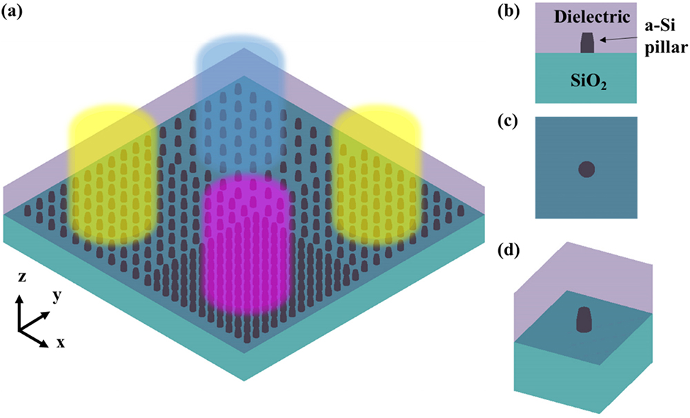
    Fig. 1. Schematic of the metasurface-based SCF function device and single nanopillar as metasurface unit cell. (a) Schematic of the SCF illustrating the color filter effect (drawing not to scale). (b) Side view, (c) top view, and (d) perspective view of the a-Si nanopillar on glass wafer for SCF design and simulation.
    Fabricated glass wafer, single dies, and single nanopillars with different heights. (a) Photo image of 300-mm glass wafer, with blue dotted line highlighting the central die. (b)–(d) Photo images of central die (from different wafers) after wafer dicing with a-Si pillar height design of (b) 110 nm, (c) 170 nm, and (d) 230 nm, respectively. Each die has a size of 26 mm × 33 mm. SCF device is highlighted using blue dotted line in each die, showing different displayed colors under different pillar heights. (e)–(g) Transmission electron microscopy (TEM) images of the fabricated a-Si nanopillar with height close to (e) 110 nm, (f) 170 nm, and (g) 230 nm.
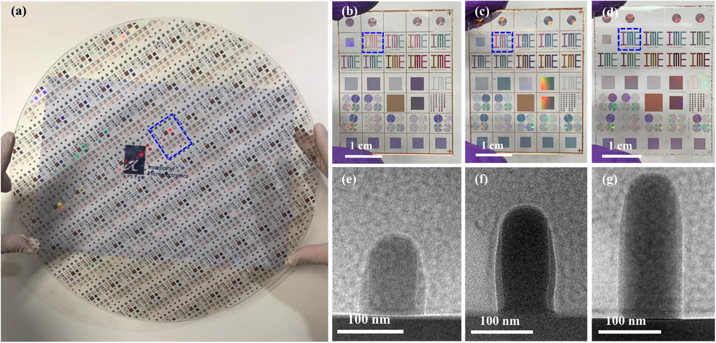
    Fig. 2. Fabricated glass wafer, single dies, and single nanopillars with different heights. (a) Photo image of 300-mm glass wafer, with blue dotted line highlighting the central die. (b)–(d) Photo images of central die (from different wafers) after wafer dicing with a-Si pillar height design of (b) 110 nm, (c) 170 nm, and (d) 230 nm, respectively. Each die has a size of 26 mm × 33 mm. SCF device is highlighted using blue dotted line in each die, showing different displayed colors under different pillar heights. (e)–(g) Transmission electron microscopy (TEM) images of the fabricated a-Si nanopillar with height close to (e) 110 nm, (f) 170 nm, and (g) 230 nm.
    Simulation and experiment results of SCF with different pillar heights and pitches. (a)–(i) Simulated (red line) and measured (blue line) transmittance spectra of the color logo “IME” under various pillar heights (H) and pitches (P) of (a) H=110 nm, P=250 nm; (b) H=170 nm, P=250 nm; (c) H=230 nm, P=250 nm; (d) H=110 nm, P=300 nm; (e) H=170 nm, P=300 nm; (f) H=230 nm, P=300 nm; (g) H=110 nm, P=350 nm; (h) H=170 nm, P=350 nm; and (i) H=230 nm, P=350 nm. Insets show the displayed color of the metasurface design. Display contrast increases as pillar height increases. The displayed colors are verified by mapping the complementarity of the filtered colors from spectra within the RYB color wheel, which are also included as insets. (j)–(l) Simulated (red marks) and measured (blue marks) CIE xy chromaticity coordinates of transmittance spectra with a-Si pillar height of (j) 110 nm, (k) 170 nm, and (l) 230 nm. For each pillar height, round, square, and rhombus shaped marks are used to represent pitches of 250 nm, 300 nm, and 350 nm, respectively.
    Fig. 3. Simulation and experiment results of SCF with different pillar heights and pitches. (a)–(i) Simulated (red line) and measured (blue line) transmittance spectra of the color logo “IME” under various pillar heights (H) and pitches (P) of (a) H=110  nm, P=250  nm; (b) H=170  nm, P=250  nm; (c) H=230  nm, P=250  nm; (d) H=110  nm, P=300  nm; (e) H=170  nm, P=300  nm; (f) H=230  nm, P=300  nm; (g) H=110  nm, P=350  nm; (h) H=170  nm, P=350  nm; and (i) H=230  nm, P=350  nm. Insets show the displayed color of the metasurface design. Display contrast increases as pillar height increases. The displayed colors are verified by mapping the complementarity of the filtered colors from spectra within the RYB color wheel, which are also included as insets. (j)–(l) Simulated (red marks) and measured (blue marks) CIE xy chromaticity coordinates of transmittance spectra with a-Si pillar height of (j) 110 nm, (k) 170 nm, and (l) 230 nm. For each pillar height, round, square, and rhombus shaped marks are used to represent pitches of 250 nm, 300 nm, and 350 nm, respectively.
    Simulated electric and magnetic fields of nanopillar under different pillar heights. (a)–(c) Electric and magnetic field distributions at resonance wavelengths of (a) 550 nm, (b) 572 nm, and (c) 580 nm for a-Si nanopillars with heights of 110, 170, and 230 nm, respectively. Pillar pitch and bottom diameter are fixed at 250 and 105 nm, respectively. The wavelengths are selected based on the resonance of the transmittance spectra from simulation shown in Figs. 3(a)–3(c). First row shows the field in the x−y plane (top view). Second row shows the field distribution in y−z plane and x−z plane for electric field and magnetic field, respectively (side view). Note: In simulation the launched light source is polarized in y direction.
    Fig. 4. Simulated electric and magnetic fields of nanopillar under different pillar heights. (a)–(c) Electric and magnetic field distributions at resonance wavelengths of (a) 550 nm, (b) 572 nm, and (c) 580 nm for a-Si nanopillars with heights of 110, 170, and 230 nm, respectively. Pillar pitch and bottom diameter are fixed at 250 and 105 nm, respectively. The wavelengths are selected based on the resonance of the transmittance spectra from simulation shown in Figs. 3(a)–3(c). First row shows the field in the xy plane (top view). Second row shows the field distribution in yz plane and xz plane for electric field and magnetic field, respectively (side view). Note: In simulation the launched light source is polarized in y direction.
    Simulation results of SCF with pillar height of 230 nm under different pillar diameters (D) and pitches (P). The filtered wavelength is able to cover the whole visible wavelength regime under D and P variation.
    Fig. 5. Simulation results of SCF with pillar height of 230 nm under different pillar diameters (D) and pitches (P). The filtered wavelength is able to cover the whole visible wavelength regime under D and P variation.
    Schematic of microscopic spectrometer measurement system.
    Fig. 6. Schematic of microscopic spectrometer measurement system.
    Zhengji Xu, Nanxi Li, Yuan Dong, Yuan Hsing Fu, Ting Hu, Qize Zhong, Yanyan Zhou, Dongdong Li, Shiyang Zhu, Navab Singh. Metasurface-based subtractive color filter fabricated on a 12-inch glass wafer using a CMOS platform[J]. Photonics Research, 2021, 9(1): 13
    Download Citation