
Guillaume Marcaud, Samuel Serna, Karamanis Panaghiotis, Carlos Alonso-Ramos, Xavier Le Roux, Mathias Berciano, Thomas Maroutian, Guillaume Agnus, Pascal Aubert, Arnaud Jollivet, Alicia Ruiz-Caridad, Ludovic Largeau, Nathalie Isac, Eric Cassan, Sylvia Matzen, Nicolas Dubreuil, Michel Rérat, Philippe Lecoeur, Laurent Vivien. Third-order nonlinear optical susceptibility of crystalline oxide yttria-stabilized zirconia[J]. Photonics Research, 2020, 8(2): 110
- Photonics Research
- Vol. 8, Issue 2, 110 (2020)
![Variation of the third-order susceptibility tensorial components (χiiii,iijj) of YSZ 3.2% in Y2O3 as a function of the relative position between Y dopants (yellow spheres) and O vacancies (green spheres). The unit cells [25] of each configuration considered, representing symmetry in equivalent vacancy/dopant distributions, are schematically given at the right. Solid lines represent the corresponding susceptibility components of c-ZrO2. All values have been computed at the PBE0 level of theory.](/richHtml/prj/2020/8/2/02000110/img_001.jpg)
Fig. 1. Variation of the third-order susceptibility tensorial components (χ i i i i , i i j j Y 2 O 3 c - ZrO 2
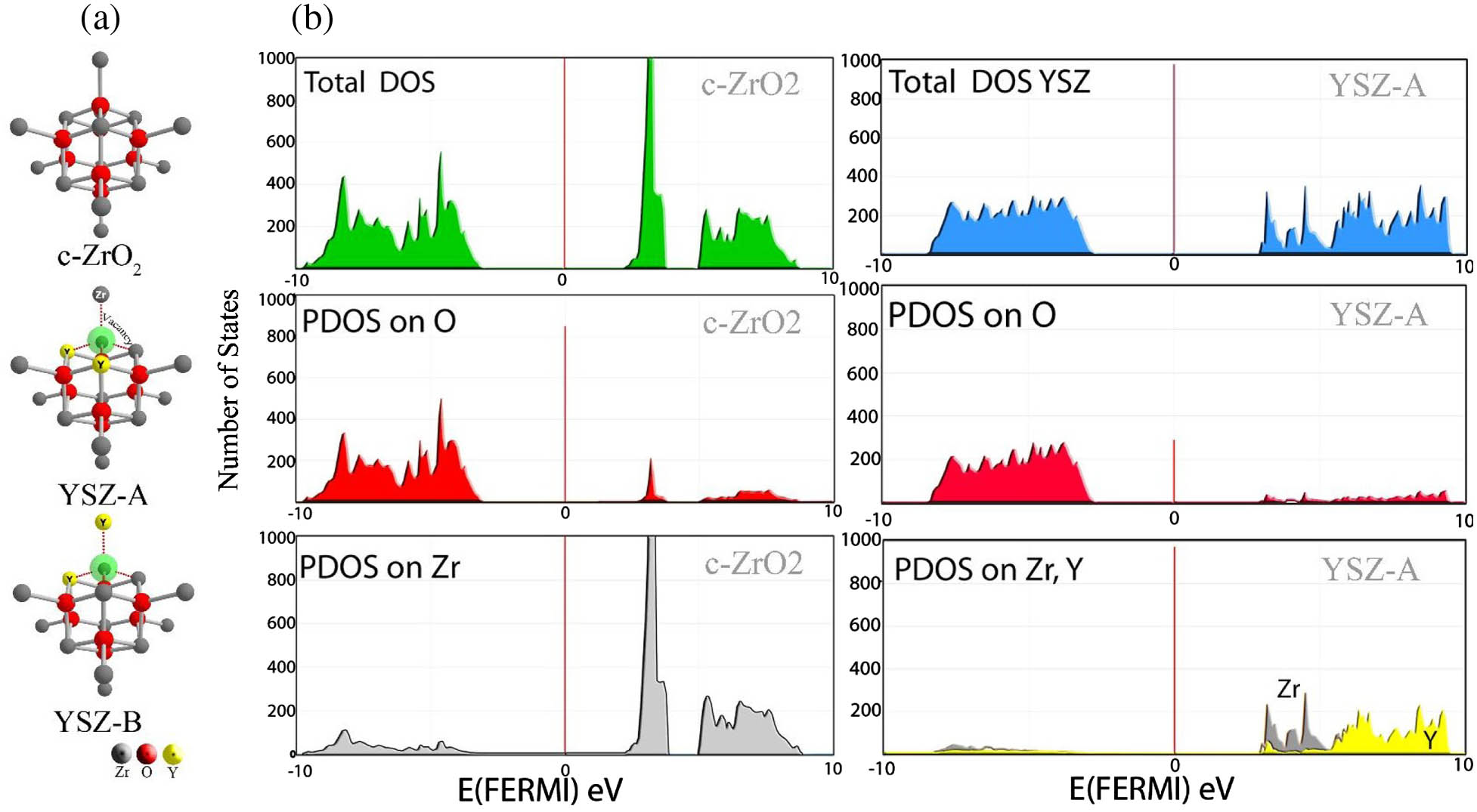
Fig. 2. (a) Symmetry nonequivalent local crystal structures of YSZ 33% in Y 2 O 3 Data File 1 and Data File 2 for the unit-cell fractional coordinates of YSZ-A and YSZ-B, respectively. (b) Total and projected density of states of c - ZrO 2
Fig. 3. (a) Unit cell of YSZ 7% considered in this study. (b) Evolution of χ i i i i ( 3 ) χ i i j j ( 3 ) Y 2 O 3 Data File 3 and Data File 4 for the unit-cell fractional coordinates of YSZ 7% and YSZ 14%, respectively.
Fig. 4. (a) Schematic view of a YSZ-based rib waveguide, designed and fabricated for single-mode quasi-TE propagation in the H = 300 nm D = 80 nm W = 760 nm 2 θ − ω ω FWHM = 0.03 ° α = 3.2 dB · cm − 1 λ = 1550 nm
Fig. 5. (a) P out P in λ = 1580 nm E g > 5 eV
Fig. 6. Waveguides facets obtained with the two-step dicing procedure, including classical dicing technique and focus ion-beam (FIB) etching. (a) Top view of the sample edges with optical microscopy and (b) cross-section observation of a waveguide facet by SEM. Whereas the first classical technique allows to mechanically dice the whole sample, the FIB technique etches a small area, here the extremities of the waveguides, leaving highly transmissive facets.
Fig. 7. Most stable structures of Zr 4 O 8 Zr 8 O 16 Zr 15 O 30
|
Table 1. Cell Parameter
|
Table 2. Unit Cell Volume V (2 )a
|
Table 3. Electronic Contribution to the Dielectric Susceptibilities (3(a) ] Computed at the PBE0 and B3LYP Levels of Theory on PBE0 Optimized Local Crystal Structuresa

Set citation alerts for the article
Please enter your email address
© Copyright 2018-2021 | Chinese Laser Press. All Rights Reserved 沪ICP备15018463号-20