
Yifan Wang, Xuanze Li, Pei Liu, Jing Xia, Xiangmin Meng. Epitaxial growth of CsPbBr3/PbS single-crystal film heterostructures for photodetection[J]. Journal of Semiconductors, 2021, 42(11): 112001
- Journal of Semiconductors
- Vol. 42, Issue 11, 112001 (2021)
Abstract
1. Introduction
Semiconductor heterostructures designed by high crystallization materials expand the application for modern microelectronics and optoelectronics with interesting properties[
All-inorganic cesium lead halide perovskite (CsPbX3, X = Cl, Br, I) has attracted significant exploration in optoelectronic applications, such as photodetectors[
In this study, we report high-quality CsPbBr3/PbS single-crystal film heterostructures through a two-step vapor phase epitaxy route, where orthorhombic CsPbBr3 single-crystal films epitaxially grow on cubic PbS(100) thin films. X-ray diffraction (XRD) and electron back-scatter diffraction (EBSD) were used to characterize the crystal structures and epitaxial relationships of the as-prepared heterostructures. CsPbBr3/PbS heterostructures reveal broadband light absorption and well-photogenerated electron transfer, which were confirmed by absorption and PL spectra. Owing to its unique optoelectronic properties, photodetectors based on the CsPbBr3/PbS heterostructures reveal superior responsivity, high detectivity, fast response speed and obvious rectification behavior.
2. Experimental section/methods
2.1. Growth and transfer for PbS single-crystal films
PbS single-crystal films were first grown on NaCl (100) crystals by the chemical vapor deposition method in a quartz tube furnace. In a typical growth, 30 mg PbCl2 powder (99.95%, Alfa Aesar) and 0.5 g sulfur powder (99.95%, Alfa Aesar) were used as sources. Then, a freshly cleaved NaCl (100) crystal as the substrate was positioned on the PbCl2 powder with the surface facing down. The PbCl2 powder was placed in the center of the tube and the sulfur powder was located approximately 20 cm upstream from the heating center. Before heating, the tube was pumped down to expel the air and then purged with high-purity Ar gas. The heating center was then ramped to 580 °C with the heating rate of 30 °C/min and kept for 15 min. Finally, the tube furnace was cooled down to room temperature naturally. During the growth, a 50 sccm Ar gas was used as the carrier. Owing to the high solubility of alkali salts, epitaxial PbS films can be transferred onto SiO2/Si substrates and can maintain good integrity and crystallinity. Then the as-grown PbS films were used as the temple of CsPbBr3 epitaxial growth.
2.2. Epitaxial growth of CsPbBr3/PbS single-crystal film heterostructures
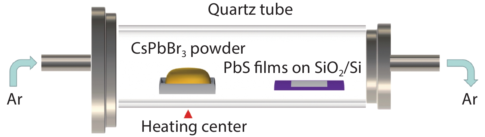
The CsPbBr3/PbS single-crystal film heterostructures were synthesized on SiO2/Si substrates through a two-step growth process in a 1 inch diameter quartz heated by a high-temperature horizontal tube furnace. For CsPbBr3/PbS single-crystal film heterostructure growth, the CsPbBr3 powder, which was synthesized via a solution-processed method[
![]()
Figure 1.(Color online) Schematic diagram of the tube furnace setup for the growth of CsPbBr3/PbS heterostructures.
2.3. Device fabrication and performance measurement
Morphologies of the sample were characterized using a Hitachi S4800 field emission scanning electron microscope. EBSD data collection was conducted in a JEOL 6500 SEM. XRD patterns were recorded via a Bruker D 8 Focus powder X-ray diffractometer using Cu Kα radiation (λ = 1.5418 Å). PL measurements were performed in a Nikon Eclipse Ti-U Inverted Microscope with a Princeton SP 2358 spectrometer and a405 nm laser was adopted as the excitation source. Steady-state absorption spectra were obtained by a Cary 5000 Ultraviolet-visible-near infrared spectrophotometer with circularlypolarized lamplight and controlled incident light using a polarizer plate.
Photodetectors based on CsPbBr3/PbS heterostructures were fabricated on the SiO2/Si substrates, which were pre-deposited Au electrodes. A copper grid shadow mask with a 200 mesh grid was covered on the surface of SiO2/Si substrates, followed by thermal evaporation of 100 nm Au as the electrodes. Then, the devices were annealed at 250 °C for 2 h in Ar atmosphere to reduce the contact resistance. Photoelectric characterizations were carried out using a Lakeshore probe station and a Keithley-4200 SCS semiconductor parameter analyzer with 450, 532, 785 and 1550 nm laser illumination under atmosphere environment.
3. Results and discussion
PbS has a NaCl-type structure with a unit cell thickness of 0.594 nm along the [001] direction, which is close to that of NaCl crystal (0.564 nm). From the small lattice mismatch (~5.3%), it can be well inferred that PbS can grow into a single-crystal film on the NaCl-type substrate. Fig. 2(a) displays that the as-synthesized PbS films have a smooth surface with little concave textures, suggesting the growth of the PbS films followed the Volmer–Weber mode. The XRD patterns of PbS films on NaCl (100) are shown in Fig. 2(b). The well-defined peaks located at 30.1° and 62.5° were readily assigned to (200) and (400) planes of cubic PbS by comparing with the standard JCPDS card of PDF#05-0592. The other two peaks related to NaCl can be readily assigned to NaCl (200) and (400) planes (JPCDS, PDF#05-0628). There are only four peaks in the XRD patterns, indicating that there is no other additional phase in PbS films as well as lattice-matching between epilayers and substrates.
![]()
Figure 2.(Color online) (a) SEM image of PbS single-crystal films epitaxially grown on NaCl (100) substrates. (b) XRD patterns of the PbS films on NaCl (100) crystals (red) and reference data (JPCDS, PDF#05-0592, black).
Subsequently, the pre-synthesized PbS films were transferred to SiO2/Si substrates and used as the receiving substrates for the epitaxial growth of CsPbBr3/PbS film heterostructures. Representative cross-section and top-view scanning electron microscope (SEM) images of the CsPbBr3/PbS films are displayed in Figs. 3(a) and 3(b). It can be seen that the as-grown heterostructures have a clear interface and both the upper CsPbBr3 and lower PbS films demonstrate uniformity and conformal characteristics. Some nucleation points were remained on the surface, indicating a typical Volmer–Weber growth process during the epitaxy of CsPbBr3 films as well. XRD results provide further evidence for the crystallographic orientation and crystallinity of the as-synthesized heterostructures, as shown in Fig. 3(c). The peaks related to cubic PbS can be observed of the CsPbBr3/PbS heterostructures, proving excellent crystallinity of transferred PbS single-crystalline films. The epitaxial relationship can be determined as CsPbBr3(110) // PbS(100). In our previous work, the vapor phase epitaxial CsPbBr3 films have been proved to be an orthorhombic structure at room temperature[
![]()
Figure 3.(Color online) (a, b) Cross-section and top-view SEM images of CsPbBr3 films epitaxially grown on PbS (100) films. (c) XRD patterns of the CsPbBr3/PbS heterostructures and standard cards of CsPbBr3 and PbS. (d) Magnified XRD pattern in (a).
The orientation relation and crystal structure of CsPbBr3/PbS heterostructures were then characterized by EBSD. Figs. 4(a) and 4(b) are pole figures of the epilayer CsPbBr3 and PbS substrates. The sharp color contrast of the pole figures confirmed the high crystallinity of samples. Additionally, the measured pole figure of CsPbBr3 in (001)-oriented fits well with the result of the PbS (001)-oriented pole figure, proving the orientation relationship is CsPbBr3(110) // PbS(100), CsPbBr3[
![]()
Figure 4.(Color online) (a, b) Experimental results of pole figures from EBSD results for CsPbBr3 and PbS. (c) EBSD orientation map of the CsPbBr3 films epitaxial growth on PbS.
The spectra of UV–vis–infrared absorption and PL were used to study the absorbance and emission of the obtained single-crystal film heterostructures. Fig. 5(a) shows the absorption spectra of pure CsPbBr3 samples and CsPbBr3/PbS heterostructures which were grown under the same conditions. Compared with CsPbBr3, the heterostructures exhibit broad-spectrum absorption from the visible to mid-infrared region, which makes it an appealing material for optoelectronics[
![]()
Figure 5.(Color online) (a) UV–visible–IR absorption spectra and (b) PL spectra of pristine CsPbBr3 and CsPbBr3/PbS heterostructures.
The photodetectors based on CsPbBr3/PbS single-crystal film heterostructures were directly fabricated on SiO2/Si substrates with pre-deposition Au electrodes. The inset of Fig. 6(a) shows the schematic model of the device. The as-fabricated devices were then annealed at 250 °C in an Ar atmosphere to improve contact between heterostructures and electrodes and reduce resistance. Fig. 6(a) exhibits the current–voltage (I–V) curves of the photodetectors under 450 nm laser illumination with the light intensity varying from 0 to40 mW/cm2. In contrast to the dark current, the photocurrent
![]()
Figure 6.(Color online) Photodetector based on CsPbBr3/PbS film heterostructures. (a)
Fig. 6(b) shows the light intensity dependence of the photocurrent. By fitting the experimental data, the photocurrent can be expressed by a power-law equation
In previous studies, CsPbBr3 shows p-type conductivity without intentional doping while PbS has n-type conductivity[
![]()
Figure 7.(Color online) (a) Schematic diagram of the CsPbBr3/PbS p–n heterojunction photodetector under laser illumination. (b) Dark current and photocurrent of the CsPbBr3/PbS heterostructure detectors under a 532, 785 and 1550 nm light with a power density of 40 mW/cm2.
4. Conclusion
In summary, CsPbBr3/PbS single-crystal film heterostructures have been achieved via vapor phase epitaxy. Both the as-synthesized PbS and CsPbBr3/PbS heterostructure films have uniform surface and excellent crystallinity. The epitaxial relationship between the CsPbBr3 epilayers and PbS substrates investigated in detail using XRD and EBSD. The absorption and PL spectra have revealed wide light absorption and photogenerated electrons transfer optical properties of the heterojunctions. Photodetectors based on the CsPbBr3/PbS heterostructures exhibit good light absorption conversion efficiency, fast response speed of ~96 ms, high detectivity of ~2.65×10¹¹ Jones, superior photoresponsivity of 15 A/W, good stability and repeatability. In addition, the devices based on CsPbBr3/PbS p–n heterojunctions show a clear rectification behavior, indicating the construct of functional low-dimensional architectures and a new generation of wide-spectrum optoelectronic devices.
Acknowledgements
This work was supported by the Natural Science Foundation of China (Grant No. 11704389), Scientific Equipment Development Project and Youth Innovation Promotion Association Project of Chinese Academy of Sciences.
References
[1] J J Zhao, H H Li, Y C Qiu et al. Programmable single-crystalline PbI2 microplate arrays and their organic/inorganic heterojunctions. Adv Funct Mater, 30, 2003631(2020).
[2] X H Xia, J P Tu, Y Q Zhang et al. High-quality metal oxide core/shell nanowire arrays on conductive substrates for electrochemical energy storage. ACS Nano, 6, 5531(2012).
[3] G Iannaccone, F Bonaccorso, L Colombo et al. Quantum engineering of transistors based on 2D materials heterostructures. Nat Nanotechnol, 13, 183(2018).
[4] H Zhang, X T Jiang, Y L Wang et al. Preface to the special issue on monoelemental 2D semiconducting materials and their applications. J Semicond, 41, 080101(2020).
[5] J Yuan, T Sun, Z X Hu et al. Wafer-scale fabrication of two-dimensional PtS2/PtSe2 heterojunctions for efficient and broad band photodetection. ACS Appl Mater Interfaces, 10, 40614(2018).
[6] F Capasso. Band-gap engineering: From physics and materials to new semiconductor devices. Science, 235, 172(1987).
[7] J S Zhou, J H Yang, Z M Wei. Photodetectors based on 2D material/Si heterostructure. J Semicond, 41, 080401(2020).
[8] H Kroemer. A proposed class of hetero-junction injection lasers. Proc IEEE, 51, 1782(1963).
[9] M Feng, N Holonyak, R Chan. Quantum-well-base heterojunction bipolar light-emitting transistor. Appl Phys Lett, 84, 1952(2004).
[10] K Lee, J Li, L Cheng et al. Sub-picosecond carrier dynamics induced by efficient charge transfer in MoTe2/WTe2 van der Waals heterostructures. ACS Nano, 13, 9587(2019).
[11] P Zhang, Y W Zhang, Y Wei et al. Contact engineering for two-dimensional semiconductors. J Semicond, 41, 071901(2020).
[12] X D Duan, C Wang, J C Shaw et al. Lateral epitaxial growth of two-dimensional layered semiconductor heterojunctions. Nat Nanotechnol, 9, 1024(2014).
[13] P Caroff, J B Wagner, K A Dick et al. High-quality InAs/InSb nanowire heterostructures grown by metal-organic vapor-phase epitaxy. Small, 4, 878(2008).
[14] Y Liu, Y Huang, X F Duan. Van der Waals integration before and beyond two-dimensional materials. Nature, 567, 323(2019).
[15] D Jariwala, T J Marks, M C Hersam. Mixed-dimensional van der Waals heterostructures. Nat Mater, 16, 170(2017).
[16] S Y Zhou, B Peng. Non-volatile optical memory in vertical van der Waals heterostructures. J Semicond, 41, 072906(2020).
[17] F Qian, Y Li, S Gradečak et al. Multi-quantum-well nanowire heterostructures for wavelength-controlled lasers. Nat Mater, 7, 701(2008).
[18] A Walsh, D O Scanlon, S Y Chen et al. Self-regulation mechanism for charged point defects in hybrid halide perovskites. Angew Chem Int Ed, 54, 1791(2015).
[19] Y Gao, L Y Zhao, Q Y Shang et al. Photoluminescence properties of ultrathin CsPbCl3 nanowires on mica substrate. J Semicond, 40, 052201(2019).
[20] H M Chen, W Huang, T J Marks et al. Recent advances in multi-layer light-emitting heterostructure transistors. Small, 17, 2007661(2021).
[21] N J Huo, J Kang, Z M Wei et al. Novel and enhanced optoelectronic performances of multilayer MoS2-WS2 heterostructure transistors. Adv Funct Mater, 24, 7025(2014).
[22] Y P Wang, Z Z Chen, F Deschler et al. Epitaxial halide perovskite lateral double heterostructure. ACS Nano, 11, 3355(2017).
[23] S J Yang, K L Liu, W Han et al. Salt-assisted growth of P-type Cu9S5 nanoflakes for P-N heterojunction photodetectors with high responsivity. Adv Funct Mater, 30, 1908382(2020).
[24] J G Feng, X X Yan, Y Liu et al. Crystallographically aligned perovskite structures for high-performance polarization-sensitive photodetectors. Adv Mater, 29, 1605993(2017).
[25] Y F Wang, F Yang, X Z Li et al. Epitaxial growth of large-scale orthorhombic CsPbBr3 perovskite thin films with anisotropic photoresponse property. Adv Funct Mater, 29, 1904913(2019).
[26] X L Zhang, B Xu, J B Zhang et al. All-inorganic perovskite nanocrystals for high-efficiency light emitting diodes: Dual-phase CsPbBr3-CsPb2Br5 composites. Adv Funct Mater, 26, 4595(2016).
[27] C Liu, W Z Li, C L Zhang et al. All-inorganic CsPbI2Br perovskite solar cells with high efficiency exceeding 13%. J Am Chem Soc, 140, 3825(2018).
[28] L Huang, N J Huo, Z Q Zheng et al. Two-dimensional transition metal dichalcogenides for lead halide perovskites-based photodetectors: Band alignment investigation for the case of CsPbBr3/MoSe2. J Semicond, 41, 052206(2020).
[29] Q W Zhou, J L Duan, X Y Yang et al. Interfacial strain release from the WS2/CsPbBr3 van der waals heterostructure for 1.7 V voltage all-inorganic perovskite solar cells. Angew Chem Int Ed, 59, 21997(2020).
[30] J Jiang, X Sun, X C Chen et al. Carrier lifetime enhancement in halide perovskite via remote epitaxy. Nat Commun, 10, 4145(2019).
[31] X F Song, X H Liu, D J Yu et al. Boosting two-dimensional MoS2/CsPbBr3 photodetectors via enhanced light absorbance and interfacial carrier separation. ACS Appl Mater Interfaces, 10, 2801(2018).
[32] N J Huo, Y J Yang, J B Li. Optoelectronics based on 2D TMDs and heterostructures. J Semicond, 38, 031002(2017).
[33] Z J Li, E Hofman, J Li et al. Photoelectrochemically active and environmentally stable CsPbBr3/TiO2 core/shell nanocrystals. Adv Funct Mater, 28, 1704288(2018).
[34] Q X Zhong, M H Cao, H C Hu et al. One-pot synthesis of highly stable CsPbBr3@SiO2 core–shell nanoparticles. ACS Nano, 12, 8579(2018).
[35] C Fan, X Xu, K Yang et al. Controllable epitaxial growth of core-shell PbSe@CsPbBr3 wire heterostructures. Adv Mater, 30, 1804707(2018).
[36] Q B Liu, L H Liang, H Z Shen et al. Epitaxial growth of CsPbBr3-PbS vertical and lateral heterostructures for visible to infrared broadband photodetection. Nano Res, 14, 1(2021).
[37] Z Wei, A Perumal, R Su et al. Solution-processed highly bright and durable cesium lead halide perovskite light-emitting diodes. Nanoscale, 8, 18021(2016).
[38] X J Zhang, X X Wu, X Y Liu et al. Heterostructural CsPbX3-PbS (X = Cl, Br, I) quantum dots with tunable vis-NIR dual emission. J Am Chem Soc, 142, 4464(2020).
[39] Y D Shen, R J Chen, X C Yu et al. Gibbs-Thomson effect in planar nanowires: Orientation and doping modulated growth. Nano Lett, 16, 4158(2016).
[40] F Wang, Z X Wang, K Xu et al. Tunable GaTe-MoS2 van der Waals p-n junctions with novel optoelectronic performance. Nano Lett, 15, 7558(2015).
[41] Y H He, L Matei, H J Jung et al. High spectral resolution of gamma-rays at room temperature by perovskite CsPbBr3 single crystals. Nat Commun, 9, 1609(2018).
[42] X L Hu, H Zhou, Z Y Jiang et al. Direct vapor growth of perovskite CsPbBr3 nanoplate electroluminescence devices. ACS Nano, 11, 9869(2017).
[43] Y Pak, S Mitra, N Alaal et al. Dark-current reduction accompanied photocurrent enhancement in p-type MnO quantum-dot decorated n-type 2D-MoS2-based photodetector. Appl Phys Lett, 116, 112102(2020).
[44] Y Wen, Q S Wang, L Yin et al. Epitaxial 2D PbS nanoplates arrays with highly efficient infrared response. Adv Mater, 28, 8051(2016).

Set citation alerts for the article
Please enter your email address
© Copyright 2018-2021 | Chinese Laser Press. All Rights Reserved 沪ICP备15018463号-20