
Houbin Zhu, Qingyun Li, Huangpu Han, Zhenyu Li, Xiuquan Zhang, Honghu Zhang, Hui Hu. Hybrid mono-crystalline silicon and lithium niobate thin films [Invited][J]. Chinese Optics Letters, 2021, 19(6): 060017
- Chinese Optics Letters
- Vol. 19, Issue 6, 060017 (2021)
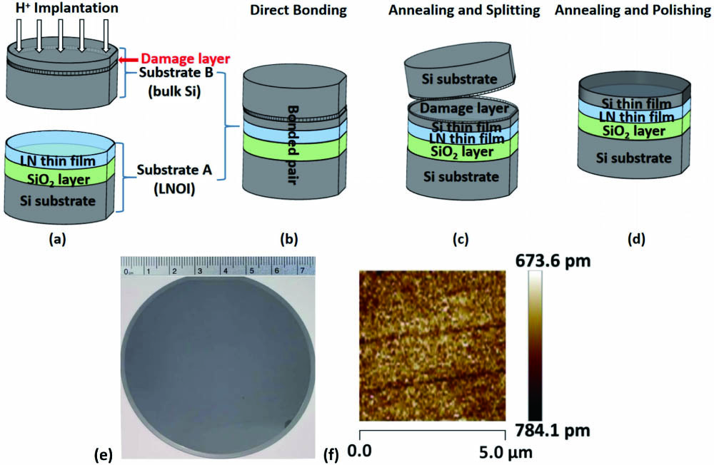
Fig. 1. Si-LNOI fabrication processes. (a) H ions were implanted into substrate B. (b) Substrates A and B were bonded by direct wafer bonding. (c) The bonded pair was annealed, and a Si thin film was split from substrate B. (d) The Si-LNOI wafer was annealed, and the surface was polished. (e) Photograph of 3 inch Si-LNOI wafer. (f) Surface roughness of Si thin film measured by AFM.
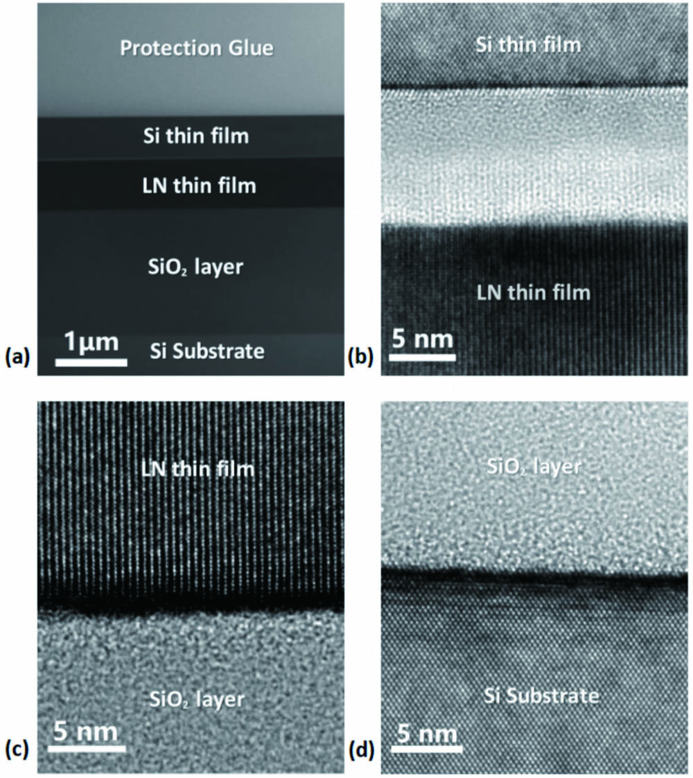
Fig. 2. (a) Cross section of Si-LNOI. (b) Interface between Si/LN thin films. (c) Interface between LN/SiO2 thin films. (d) Interface between SiO2 layer and Si substrate.
Fig. 3. H-atom concentration in Si-LNOI along the depth direction.
Fig. 4. (a) ω scans of (400) crystal planes of Si thin film and Si substrate. (b) 2θ scans of (400) crystal planes of Si thin film and bulk Si. (c) ω scan of (110) crystal plane of LN thin film. (d) The 2θ scans of (110) crystal planes of LN thin film and bulk LN.
Fig. 5. Raman spectra of bulk Si, mono-crystalline Si thin film, and a-Si thin film.
Fig. 6. (a) Optical microscopy image of Si strip-loaded waveguide with a polished end face. (b) Cross section of a waveguide measured by AFM. (c) Measured optical intensity distribution, and normalized transmission of q-TE mode in Si strip-loaded waveguide.

Set citation alerts for the article
Please enter your email address
© Copyright 2018-2021 | Chinese Laser Press. All Rights Reserved 沪ICP备15018463号-20