• Acta Optica Sinica
  • Vol. 41, Issue 4, 0413001 (2021)
Wanle Pan1, Heming Chen2、*, Yuyang Zhuang1, and Yuchen Hu1
Author Affiliations
  • 1College of Electronic and Optical Engineering & College of Microelectronics, Nanjing University of Posts and Telecommunications, Nanjing, Jiangsu 210023, China;
  • 2Bell Honors School, Nanjing University of Posts and Telecommunications, Nanjing, Jiangsu 210023, China
  • show less
    DOI: 10.3788/AOS202141.0413001 Cite this Article Set citation alerts
    Wanle Pan, Heming Chen, Yuyang Zhuang, Yuchen Hu. Hybrid Demultiplexer for Mode-Wavelength Division Based on Nanowire Waveguides and One-Dimensional Photonic Crystal Nanobeam Cavity[J]. Acta Optica Sinica, 2021, 41(4): 0413001 Copy Citation Text show less
    Working principle of MDM-WDM hybrid demultiplexer
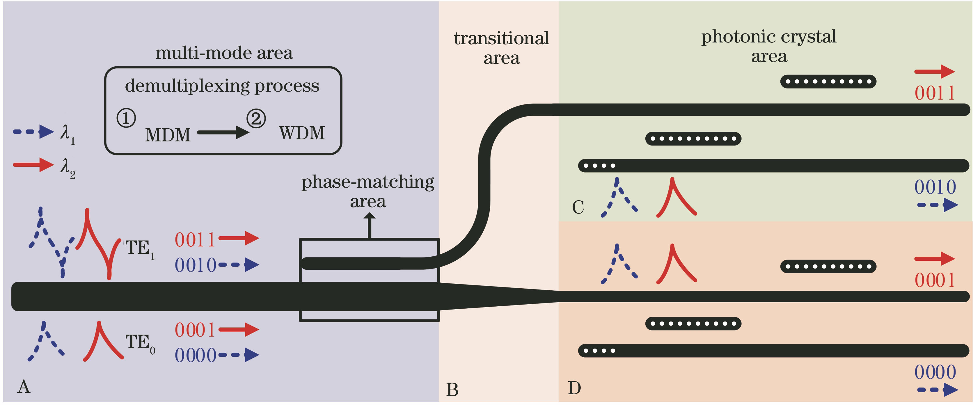
    Fig. 1. Working principle of MDM-WDM hybrid demultiplexer
    Theoretical model of WDM
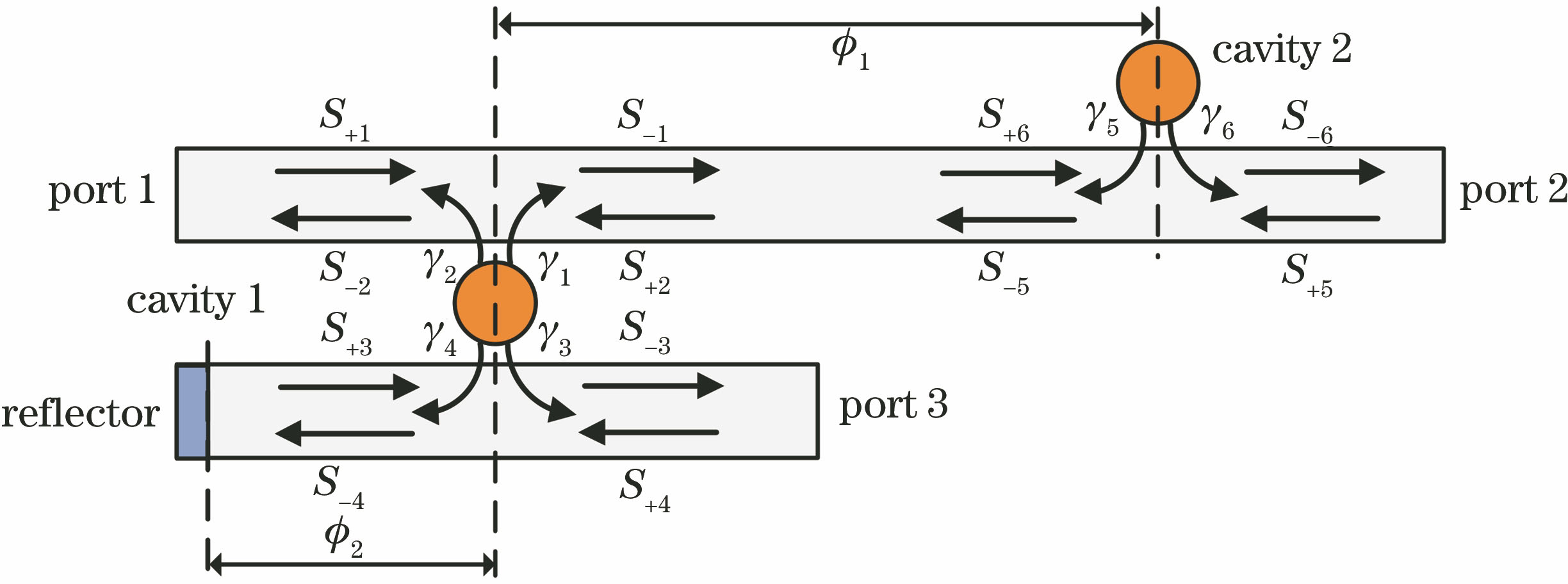
    Fig. 2. Theoretical model of WDM
    Transmission spectra of theoretical model. (a) Theoretical transmission spectra of each port; (b) local magnification of reflection spectrum
    Fig. 3. Transmission spectra of theoretical model. (a) Theoretical transmission spectra of each port; (b) local magnification of reflection spectrum
    Three-dimensional structural diagram of MDM-WDM hybrid demultiplexer
    Fig. 4. Three-dimensional structural diagram of MDM-WDM hybrid demultiplexer
    Structural parameters and static field distribution of one-dimensional photonic crystal nanobeam cavity. (a) Structural diagram; (b) hole radius distribution in microcavity area; (c) static field distribution of resonant cavity mode
    Fig. 5. Structural parameters and static field distribution of one-dimensional photonic crystal nanobeam cavity. (a) Structural diagram; (b) hole radius distribution in microcavity area; (c) static field distribution of resonant cavity mode
    Structural diagrams of WDM demultiplexer. (a) Three-dimensional; (b) two-dimensional
    Fig. 6. Structural diagrams of WDM demultiplexer. (a) Three-dimensional; (b) two-dimensional
    Transmission spectra of WDM demultiplexer. (a) Transmission spectrum at each port; (b) enlarge views of transmission spectra
    Fig. 7. Transmission spectra of WDM demultiplexer. (a) Transmission spectrum at each port; (b) enlarge views of transmission spectra
    Static field distributions of different incident light in WDM demultiplexing process. (a) 1570.0 nm; (b) 1573.2 nm
    Fig. 8. Static field distributions of different incident light in WDM demultiplexing process. (a) 1570.0 nm; (b) 1573.2 nm
    Relationship between performance of WDM demultiplexer and Δr. (a) Insertion loss at each wavelength versus Δr; (b) channel crosstalk at each wavelength versus Δr
    Fig. 9. Relationship between performance of WDM demultiplexer and Δr. (a) Insertion loss at each wavelength versus Δr; (b) channel crosstalk at each wavelength versus Δr
    Structural parameters and transmission spectra of MDM demultiplexer. (a) Effective refractive index map of nanowire waveguides; (b) three-dimensional structural diagram; (c) side view of three-dimensional structure; (d) transmission spectra; (e) different mode conversion diagrams
    Fig. 10. Structural parameters and transmission spectra of MDM demultiplexer. (a) Effective refractive index map of nanowire waveguides; (b) three-dimensional structural diagram; (c) side view of three-dimensional structure; (d) transmission spectra; (e) different mode conversion diagrams
    Relationship between performance of MDM demultiplexer and Lc. (a) Insertion loss of each mode versus Lc; (b) channel crosstalk of each mode versus Lc
    Fig. 11. Relationship between performance of MDM demultiplexer and Lc. (a) Insertion loss of each mode versus Lc; (b) channel crosstalk of each mode versus Lc
    Transmission spectra of ports O3 and O4 in demultiplexing process. (a) Hole is not fine-tuned; (b) hole is fine-tuned
    Fig. 12. Transmission spectra of ports O3 and O4 in demultiplexing process. (a) Hole is not fine-tuned; (b) hole is fine-tuned
    Transmission spectra of each mode in demultiplexing process. (a) TE0; (b) TE1
    Fig. 13. Transmission spectra of each mode in demultiplexing process. (a) TE0; (b) TE1
    Static field distribution in demultiplexing process. (a) TE0 at 1570.0 nm; (b) TE0 at 1573.2 nm; (c) TE1 at 1570.0 nm; (d) TE1 at 1573.2 nm
    Fig. 14. Static field distribution in demultiplexing process. (a) TE0 at 1570.0 nm; (b) TE0 at 1573.2 nm; (c) TE1 at 1570.0 nm; (d) TE1 at 1573.2 nm
    PortTE0TE1
    @1570.0 nm@1573.2 nm@1570.0 nm@1573.2 nm
    O30.37 dB
    O40.15 dB
    O50.37 dB
    O60.13 dB
    Table 1. Insertion loss of each mode
    PortTE0TE1
    @1570.0 nm@1573.2 nm@1570.0 nm@1573.2 nm
    O3-22.7 dB-35.8 dB-36.4 dB
    O4-19.2 dB-30.3 dB-29.8 dB
    O5-35.9 dB-32.6 dB-23.0 dB
    O6-43.7 dB-39.3 dB-18.4 dB
    Table 2. Channel crosstalk of each mode
    Wanle Pan, Heming Chen, Yuyang Zhuang, Yuchen Hu. Hybrid Demultiplexer for Mode-Wavelength Division Based on Nanowire Waveguides and One-Dimensional Photonic Crystal Nanobeam Cavity[J]. Acta Optica Sinica, 2021, 41(4): 0413001
    Download Citation