Author Affiliations
1School of Materials Science and Engineering, Guilin University of Technology, Guilin 541004, China2Center for Excellence in Nanoscience (CAS), Key Laboratory of Nanosystem and Hierarchical Fabrication (CAS), National Center for Nanoscience and Technology, Beijing 100190, China3School of Materials and Energy, Yunnan University, Kunming 650500, China4School of Materials Science and Engineering, Beihang University, Beijing 100191, Chinashow less
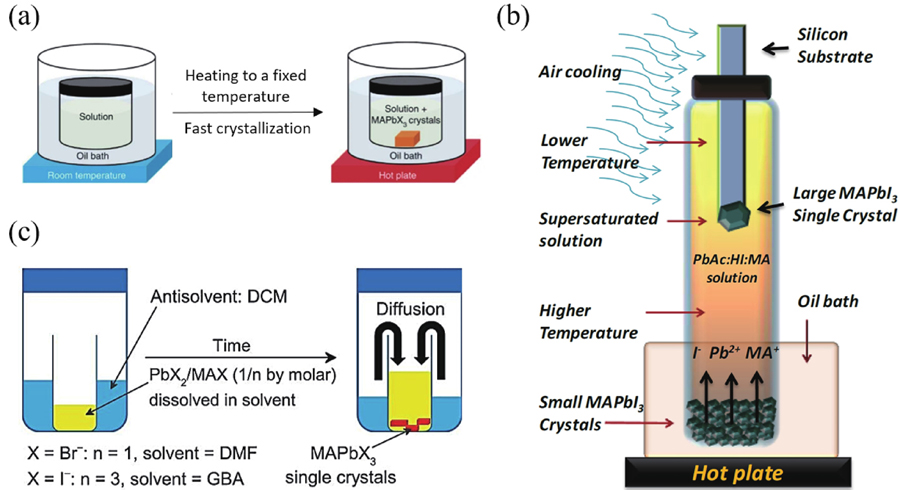
A variety of crystallization methods have been developed for preparing high-quality perovskite single crystals[17-21], including inverse temperature crystallization (ITC) method[19], solution temperature-lowering (STL) method[20,21] and antisolvent vapor-assisted crystallization (AVC) method[22,23]. ITC method was first proposed by Bakret al. to grow MAPbX3 (X = Br–, I–) single crystals in 2015[19] (Fig. 1(a)). This method is applied to precursors with inverse solubility in certain organic solvents (i.e., the solubility decreases as temperature increases). Perovskite molecules in complex can be released by raising the temperature, initiating supersaturation and crystallization. For MAPbI3, MAPbBr3 and MAPbCl3, the applicable solvents for ITC method are GBL, DMF and DMSO, respectively. This method is commonly used because it is very simple and quick. For STL method, the supersaturation is achieved by lowering the temperature of a hot saturated solution[20] (Fig. 1(b)). The solvents have increasing solubility with temperature, e.g., HI-based solution. High-quality single crystals can be obtained by precisely controlling the rate of lowering temperature[21]. However, STL method is quite time-consuming. Bakret al. reported AVC method to grow sizable MAPbX3 (X = I or Br) single crystals with volumes exceeding 100 mm3[22]. The perovskite solution was sealed in an antisolvent-containing container, and the diffusion of antisolvents induces slow and uniform crystallization without changing the temperature (Fig. 1(c)). Dinget al. utilized this method to grow lead-free perovskite materials (NH4)3Sb2IxBr9–x in ethanol solvent[23].
Single crystals of perovskites present application potential in solar cells, photodetectors and LEDs by virtue of superior optoelectronic properties. Various growth methods have been developed to obtain large single crystals with high quality. More efforts will focus on size control, interface modification and long-term stability.
Perovskite single crystals have been used in PDs. In 2015, Sunet al. first utilized perovskite single crystal to make PDs (Fig. 2(c)), revealing better performance and durability than its polycrystalline counterpart[27]. Under 1 mW/cm2 light illumination, MAPbI3 single-crystal PD showed 100 times higher responsivity and EQE. To further increase the detectivity and lower the noise, Huanget al. made detectors with thin perovskite single crystals, obtaining low dark current, low noise and high detectivity[28]. MAPbBr3 PDs offered a record linear dynamic range of 256 dB, which can be attributed to reduced carrier recombination. In 2016, Huang et al. first explored the application of MAPbBr3 single crystal in X-ray detector, achieving a high mobility-lifetime product of 1.2 × 10⁻² cm2/V[29]. Lead-free perovskite single crystals were also used in X-ray detectors. Tanget al. used double perovskite Cs2AgBiBr6 single crystal to make X-ray detectors with a minimum detectable dose rate of 59.7 nGyair/s[30]. Yanget al. reported anisotropic X-ray detectors based on (NH4)3Bi2I9 single crystals with a detection limit as low as 55 nGyair/s[31]. Liuet al. used refinement solution to get rid of extraneous nuclei and grew large Cs3Bi2I9 single crystals[32]. The X-ray detectors showed high sensitivity, low dark current and high thermal stability at 100 °C, being suitable for X-ray imaging (Fig. 2(d)).
![(Color online) Common solution growth methods for perovskite single crystals. (a) Inverse temperature crystallization method. Reproduced with permission[19], Copyright 2015, Springer Nature. (b) Solution temperature-lowering method. Reproduced with permission[20], Copyright 2015, Science (AAAS). (c) Antisolvent vapor-assisted crystallization. Reproduced with permission[22], Copyright 2015, Science (AAAS).](/Images/icon/loading.gif)
Figure 1.(Color online) Common solution growth methods for perovskite single crystals. (a) Inverse temperature crystallization method. Reproduced with permission[19], Copyright 2015, Springer Nature. (b) Solution temperature-lowering method. Reproduced with permission[20], Copyright 2015, Science (AAAS). (c) Antisolvent vapor-assisted crystallization. Reproduced with permission[22], Copyright 2015, Science (AAAS).
Moreover, perovskite single crystal can be a good electroluminescent material. Yuet al. first reported LEDs based on MAPbBr3 single-crystal micro-platelets with a simple structure ITO/PVK/Au[33]. The device emitted green light with a luminance of ~5000 cd/m2, lasting for at least 54 h without degradation (Fig. 2(e)). Then, the electroluminescence blinking behavior of MAPbBr3 single crystal was observed. The device with a structure ITO/MAPbBr3/ITO exhibited a low operation voltage of 2 V and a pure green emission with full width at half maximum of ~20 nm[34]. Nevertheless, the luminescence went through blinking at the crystal edges. The radiative recombination mainly occurred at crystal edges due to spatial confinement effect, but large number of traps and defects also exist at the edges, providing non-radiative paths. The excitons either emitted light or were quenched by the traps at the edges, leading to blinking. Yanget al. prepared a series of 2D Ruddlesden-Popper perovskite single crystals with the formula of (BA)2Csn−1PbnBr3n+1[35]. Blue LEDs with high color purity were madevia a micromechanical exfoliation method. The emission can be tuned across blue light range by varyingn (Fig. 2 (f)).
For photovoltaic application, the absence of grain boundary in single crystals lowers the defect density and increases carrier diffusion length, theoretically enabling better device performance. While in practice, it is challenging to obtain single-crystal devices with controllable thickness, negligible surface defects and well-deposited functional layers, which explains their underperformance compared with polycrystalline counterparts. Efforts have been made to thickness control, defect engineering and interface management, pushing the power conversion efficiency (PCE) to over 20%. Bakret al. used space-limited ITC method to grow size-controllable MAPbI3 single crystal[24]. A PTAA-coated substrate was used to cover another PTAA-coated substrate spread with perovskite precursor on the surface, and the complex was then heated slowly. The growth of crystal film was confined by hydrophobic substrates, and micrometers-thick single-crystal film was obtained. With careful separation of two substrates with a blade, good contact between crystal film and transport layer could be ensured, yielding a PCE of 21.09% with a high fill factor of 84.3%. To reduce surface defects caused by MAI escape at high temperature, Bakret al. lowered the crystallization temperature by using mixed solvent, propylene carbonate (PC) and GBL[25] (Fig. 2(a)). The addition of PC can let crystallization to occur at <90 °C. The film exhibited a smooth surface with a uniform thickness of ~20μm (Fig. 2(b)). The PCE was increased to 21.9%. To further broaden near-infrared (NIR) response, mixed-cation FA0.6MA0.4PbI3 single-crystal films were made[26]. The external quantum efficiency (EQE) spectra showed edge redshifted, increasing short-circuit current density to over 26 mA/cm2 while maintaining the open-circuit voltage. A PCE of 22.8% was achieved.
Figure 2.(Color online) (a) MAI escape from MAPbI3 films in high-temperature and low-temperature crystallization. (b) Cross-sectional SEM images and device structure for MAPbI3 single-crystal PSC. Reproduced with permission[25], Copyright 2020, American Chemical Society. (c) The planar-type photodetector fabricated on (100) facet of a MAPbI3 single crystal. Reproduced with permission[27], Copyright 2015, Springer Nature. (d) The X-ray image for a key by Cs3Bi2I9 single-crystal detector (1 × 1 mm2). Reproduced with permission[32], Copyright 2020, Springer Nature. (e) Emission intensityvs time plot for an LED operated at 1 mA current. Inset: SEM image for MAPbBr3 micro-platelet and the image of LED att = 12 h. Reproduced with permission[33], Copyright 2017, American Chemical Society. (f) Normalized PL spectra for (BA)2Csn−1PbnBr3n+1 single crystals. Reproduced with permission[35], Copyright 2020, Science (AAAS).
During last decade, metal halide perovskites (MHPs) have become research hotspot due to their superior optoelectronic properties[1-15]. MHP single crystal was first reported in 1978[16]. Up to now, MHP single crystals with various compositions have been synthesized and characterized. Compared with perovskite polycrystalline films, perovskite single crystals show lower defect density, higher carrier mobility, longer carrier diffusion length. Here, we summarize the growth methods of perovskite single crystals, and discuss their optoelectronic applications, including perovskite solar cells (PSCs), photodetectors (PDs) and light-emitting diodes (LEDs).
References
[1] L Li, H Y Chen, Z M Fang et al. An electrically modulated single-color/dual-color imaging photodetector. Adv Mater, 32, 1907257(2020).
[2] D W Zhao, L M Ding. All-perovskite tandem structures shed light on thin-film photovoltaics. Sci Bull, 65, 1144(2020).
[3] C T Zuo, L M Ding. Drop-casting to make efficient perovskite solar cells under high humidity. Angew Chem Int Ed, 60, 11242(2021).
[4] Y H Cheng, L M Ding. Pushing commercialization of perovskite solar cells by improving their intrinsic stability. Energy Environ Sci, 14, 3233(2021).
[5] H Y Xiang, C T Zuo, H B Zeng et al. White light-emitting diodes from perovskites. J Semicond, 42, 030202(2021).
[6] S R Wang, A L Wang, F Hao et al. Renaissance of tin halide perovskite solar cells. J Semicond, 42, 030201(2021).
[7] L Liu, Z Xiao, C T Zuo et al. Inorganic perovskite/organic tandem solar cells with efficiency over 20%. J Semicond, 42, 020501(2021).
[8] M Q Zhang, C T Zuo, J J Tian et al. Blue perovskite LEDs. J Semicond, 42, 070201(2021).
[9] Z W Ma, G J Xiao, L M Ding. Pressure-induced emission from low-dimensional perovskites. J Semicond, 42, 100203(2021).
[10] H Zhou, H Wang, L M Ding. Perovskite nanowire networks for photodetectors. J Semicond, 42, 110202(2021).
[11] M B Li, J J Zhou, H Tan et al. Multifunctional succinate additive for flexible perovskite solar cells with more than 23% power-conversion efficiency. The Innovation, 3, 100310(2022).
[12] L Y Mei, H R Mu, L Zhu et al. Frontier applications of perovskites beyond photovoltaics. J Semicond, 43, 040203(2022).
[13] X Y Pan, L M Ding. Application of metal halide perovskite photodetectors. J Semicond, 43, 020203(2022).
[14] L X Zhang, X Y Pan, L Liu et al. Star perovskite materials. J Semicond, 43, 030203(2022).
[15] S Y Wang, L G Tan, J J Zhou et al. Over 24% efficient MA-free Cs xFA 1– xPbX 3 perovskite solar cells. Joule, 6, 1344(2022).
[16] D Weber. CH 3NH 3SnBr xI 3– x( x = 0–3), a Sn(II)-system with cubic perovskite structure. Z Naturforsch B, 33, 862(1978).
[17] L L Ke, L M Ding. Perovskite crystallization. J Semicond, 42, 080203(2021).
[18] Y L Li, L M Ding. Single-crystal perovskite devices. Sci Bull, 66, 214(2021).
[19] M I Saidaminov, A L Abdelhady, B Murali et al. High-quality bulk hybrid perovskite single crystals within minutes by inverse temperature crystallization. Nat Commun, 6, 7586(2015).
[20] Q F Dong, Y J Fang, Y C Shao et al. Electron-hole diffusion lengths > 175 µm in solution-grown CH 3NH 3PbI 3 single crystals. Science, 347, 967(2015).
[21] Y Y Dang, Y Liu, Y X Sun et al. Bulk crystal growth of hybrid perovskite material CH 3NH 3PbI 3. CrystEngComm, 17, 665(2015).
[22] D Shi, V Adinolfi, R Comin et al. Low trap-state density and long carrier diffusion in organolead trihalide perovskite single crystals. Science, 347, 519(2015).
[23] C T Zuo, L M Ding. Lead-free perovskite materials (NH 4) 3Sb 2- I xBr 9– x. Angew Chem Int Ed, 56, 6528(2017).
[24] Z L Chen, B Turedi, A Y Alsalloum et al. Single-crystal MAPbI 3 perovskite solar cells exceeding 21% power conversion efficiency. ACS Energy Lett, 4, 1258(2019).
[25] A Y Alsalloum, B Turedi, X P Zheng et al. Low-temperature crystallization enables 21.9% efficient single-crystal MAPbI 3 inverted perovskite solar cells. ACS Energy Lett, 5, 657(2020).
[26] A Y Alsalloum, B Turedi, K Almasabi et al. 22.8%-Efficient single-crystal mixed-cation inverted perovskite solar cells with a near-optimal bandgap. Energy Environ Sci, 14, 2263(2021).
[27] Z P Lian, Q F Yan, Q R Lv et al. High-performance planar-type photodetector on (100) facet of MAPbI 3 single crystal. Sci Rep, 5, 16563(2015).
[28] C X Bao, Z L Chen, Y J Fang et al. Low-noise and large-linear-dynamic-range photodetectors based on hybrid-perovskite thin-single-crystals. Adv Mater, 29, 1703209(2017).
[29] H T Wei, Y J Fang, P Mulligan et al. Sensitive X-ray detectors made of methylammonium lead tribromide perovskite single crystals. Nat Photonics, 10, 333(2016).
[30] W C Pan, H D Wu, J J Luo et al. Cs 2AgBiBr 6 single-crystal X-ray detectors with a low detection limit. Nat Photonics, 11, 726(2017).
[31] R Z Zhuang, X J Wang, W B Ma et al. Highly sensitive X-ray detector made of layered perovskite-like (NH 4) 3Bi 2I 9 single crystal with anisotropic response. Nat Photonics, 13, 602(2019).
[32] Y X Zhang, Y C Liu, Z Xu et al. Nucleation-controlled growth of superior lead-free perovskite Cs 3Bi 2I 9 single-crystals for high-performance X-ray detection. Nat Commun, 11, 2304(2020).
[33] M M Chen, X Shan, T Geske et al. Manipulating ion migration for highly stable light-emitting diodes with single-crystalline organometal halide perovskite microplatelets. ACS Nano, 11, 6312(2017).
[34] V C Nguyen, H Katsuki, F Sasaki et al. Single-crystal perovskite CH 3NH 3PbBr 3 prepared by cast capping method for light-emitting diodes. Jpn J Appl Phys, 57, 04FL10(2018).
[35] H Chen, J Lin, J Kang et al. Structural and spectral dynamics of single-crystalline Ruddlesden-Popper phase halide perovskite blue light-emitting diodes. Sci Adv, 6, eaay4045(2020).