• Photonics Research
  • Vol. 8, Issue 3, 318 (2020)
Paul Hill1、2, Charalambos Klitis3, Benoit Guilhabert1, Marc Sorel3, Erdan Gu1, Martin D. Dawson1, and Michael J. Strain1、*
Author Affiliations
  • 1Institute of Photonics, Department of Physics, Technology and Innovation Centre, University of Strathclyde, Glasgow G1 1RD, UK
  • 2Diamond Science and Technology, Centre for Doctoral Training, University of Warwick, Coventry CV4 7AL, UK
  • 3School of Engineering, University of Glasgow, Glasgow G12 8LT, UK
  • show less
    DOI: 10.1364/PRJ.372358 Cite this Article Set citation alerts
    Paul Hill, Charalambos Klitis, Benoit Guilhabert, Marc Sorel, Erdan Gu, Martin D. Dawson, Michael J. Strain. All-optical tuning of a diamond micro-disk resonator on silicon[J]. Photonics Research, 2020, 8(3): 318 Copy Citation Text show less
    Schematic of a hybrid integration scheme where diamond micro-disk resonators are fabricated separately from a host photonic integrated circuit chip. The fully fabricated diamond resonators are transferred onto the silicon photonic chip using a high-accuracy transfer printing method.
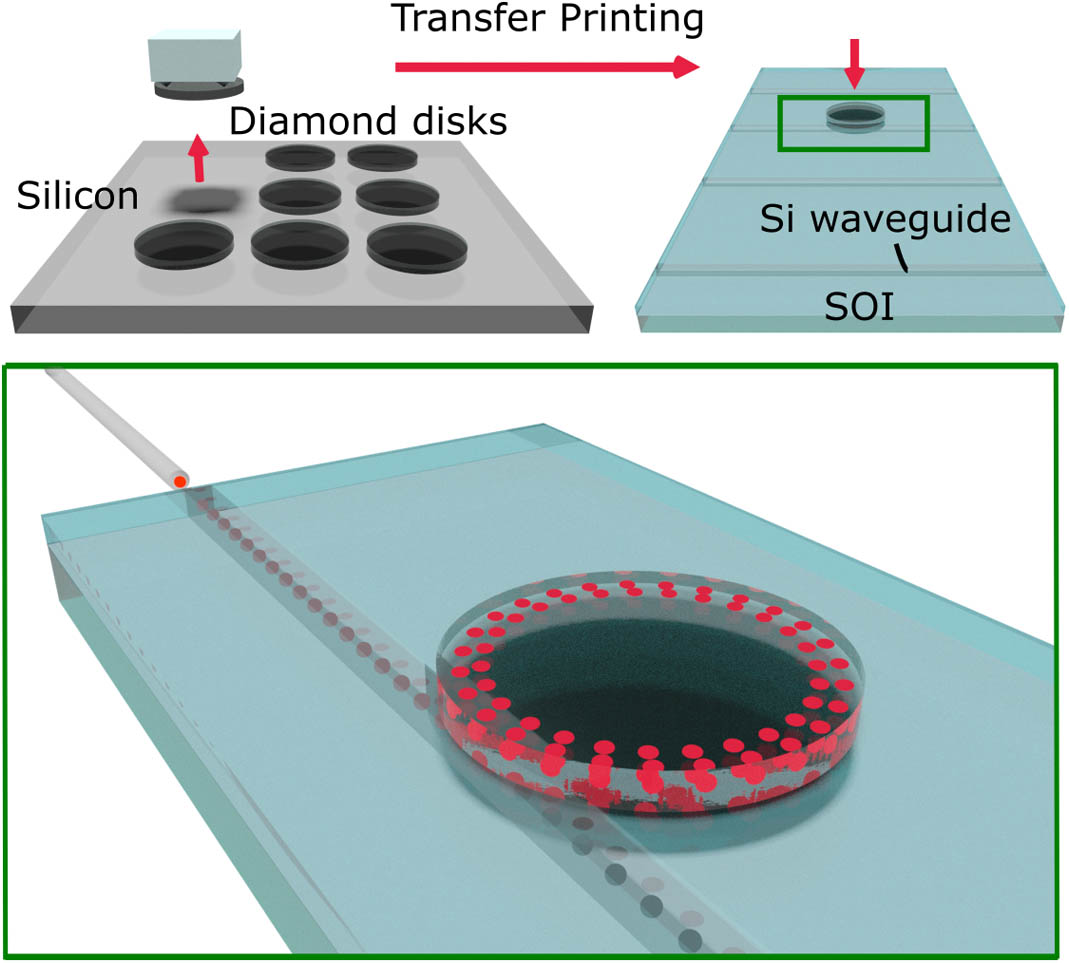
    Fig. 1. Schematic of a hybrid integration scheme where diamond micro-disk resonators are fabricated separately from a host photonic integrated circuit chip. The fully fabricated diamond resonators are transferred onto the silicon photonic chip using a high-accuracy transfer printing method.
    (a) Schematic of a wedged diamond sample, (b) patterned devices illustrating device thickness selection using an iterative printing and thinning process. (c) Optical micrograph of an array of tessellated squares fabricated on a wedged single crystal diamond sample. The arrows show the axes of low and high material wedge gradient.
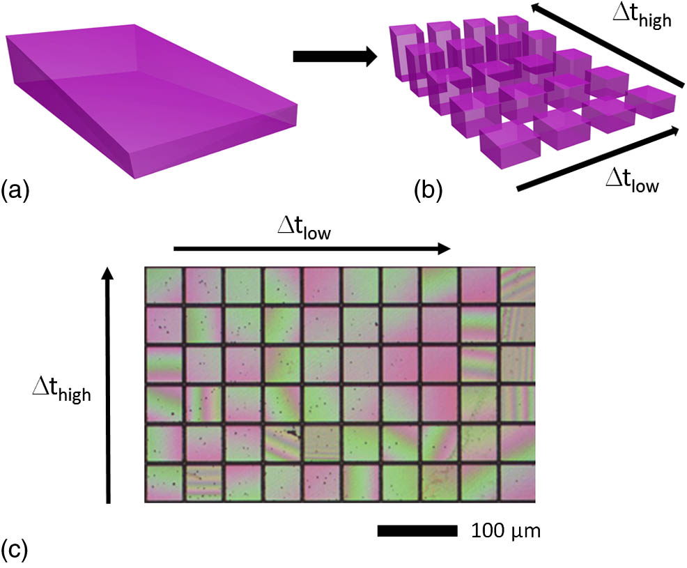
    Fig. 2. (a) Schematic of a wedged diamond sample, (b) patterned devices illustrating device thickness selection using an iterative printing and thinning process. (c) Optical micrograph of an array of tessellated squares fabricated on a wedged single crystal diamond sample. The arrows show the axes of low and high material wedge gradient.
    Transfer printing process: (a) resist is spun and (b) patterned on a diamond membrane, (c) the pattern is transferred to the diamond using inductively coupled-plasma reactive ion etching. (d)–(f) A PDMS stamp is aligned with the diamond membrane device, brought into close contact, and retracted to release the membrane. (g)–(i) The membrane is aligned over a host substrate, brought into contact, and released, leaving it transferred on the new substrate.
    Fig. 3. Transfer printing process: (a) resist is spun and (b) patterned on a diamond membrane, (c) the pattern is transferred to the diamond using inductively coupled-plasma reactive ion etching. (d)–(f) A PDMS stamp is aligned with the diamond membrane device, brought into close contact, and retracted to release the membrane. (g)–(i) The membrane is aligned over a host substrate, brought into contact, and released, leaving it transferred on the new substrate.
    (a) Two 45 deg tilted-view SEM micrographs showing eight membranes from the same original diamond sample, printed onto a silicon substrate. (b) Mean measured thickness for each of the eight membranes demonstrating the possibility of selecting membranes by their thickness, dependent on their original position on the sample.
    Fig. 4. (a) Two 45 deg tilted-view SEM micrographs showing eight membranes from the same original diamond sample, printed onto a silicon substrate. (b) Mean measured thickness for each of the eight membranes demonstrating the possibility of selecting membranes by their thickness, dependent on their original position on the sample.
    (a) Power distributions of the first three TM whispering gallery modes of a diamond disk resonator with 1.8 μm thickness printed on a silica substrate. (b) Diamond disk mode overlap with the silicon waveguide as a function of lateral offset, Δx, between the disk and waveguide.
    Fig. 5. (a) Power distributions of the first three TM whispering gallery modes of a diamond disk resonator with 1.8 μm thickness printed on a silica substrate. (b) Diamond disk mode overlap with the silicon waveguide as a function of lateral offset, Δx, between the disk and waveguide.
    Optical microscope image showing a 12.5 μm radius diamond disk integrated with a silicon waveguide using micro-transfer printing.
    Fig. 6. Optical microscope image showing a 12.5 μm radius diamond disk integrated with a silicon waveguide using micro-transfer printing.
    Optical measurement setup used for spectral characterization of the integrated micro-disk. The pump laser source, EDFA, and OSA are only used for the pump/probe thermal tuning measurements.
    Fig. 7. Optical measurement setup used for spectral characterization of the integrated micro-disk. The pump laser source, EDFA, and OSA are only used for the pump/probe thermal tuning measurements.
    Normalized transmission spectrum of the hybrid diamond–silicon micro-disk resonator.
    Fig. 8. Normalized transmission spectrum of the hybrid diamond–silicon micro-disk resonator.
    (a) Measured transmission and fit to analytic all-pass resonator function for a mode around the average loaded Q-factor of the device. (b) Measured transmission and fitted curve for the highest measured loaded Q-factor resonance. κ is the power cross-coupling coefficient, and the loss refers to the distributed propagation loss value of the resonator.
    Fig. 9. (a) Measured transmission and fit to analytic all-pass resonator function for a mode around the average loaded Q-factor of the device. (b) Measured transmission and fitted curve for the highest measured loaded Q-factor resonance. κ is the power cross-coupling coefficient, and the loss refers to the distributed propagation loss value of the resonator.
    Power cross-coupling coefficients (squares) and distributed losses (circles) as a function of measured loaded Q-factor.
    Fig. 10. Power cross-coupling coefficients (squares) and distributed losses (circles) as a function of measured loaded Q-factor.
    Transmission spectra of the diamond resonator measured using a continuously swept laser source with on-chip source power as a parameter.
    Fig. 11. Transmission spectra of the diamond resonator measured using a continuously swept laser source with on-chip source power as a parameter.
    Probe measured wavelength shift of a resonance centered at ∼1547 nm for different pump powers injected in the 1563 nm resonance. Inset: probe spectral measurements of a resonant mode at 0 mW and 4.25 mW on-chip pump powers.
    Fig. 12. Probe measured wavelength shift of a resonance centered at 1547  nm for different pump powers injected in the 1563 nm resonance. Inset: probe spectral measurements of a resonant mode at 0 mW and 4.25 mW on-chip pump powers.
    Simulation of thermal diffusion in the hybrid diamond-on-silica-on-silicon stack showing high confinement in the printed diamond micro-disk. (a) Schematic of the material stack, (b) thermal simulation close to the micro-disk region.
    Fig. 13. Simulation of thermal diffusion in the hybrid diamond-on-silica-on-silicon stack showing high confinement in the printed diamond micro-disk. (a) Schematic of the material stack, (b) thermal simulation close to the micro-disk region.
    Paul Hill, Charalambos Klitis, Benoit Guilhabert, Marc Sorel, Erdan Gu, Martin D. Dawson, Michael J. Strain. All-optical tuning of a diamond micro-disk resonator on silicon[J]. Photonics Research, 2020, 8(3): 318
    Download Citation