Abstract
High-quality integrated diamond photonic devices have previously been demonstrated in applications from non-linear photonics to on-chip quantum optics. However, the small sample sizes of single crystal material available, and the difficulty in tuning its optical properties, are barriers to the scaling of these technologies. Both of these issues can be addressed by integrating micrometer-scale diamond devices onto host photonic integrated circuits using a highly accurate micro-assembly method. In this work a diamond micro-disk resonator is integrated with a standard single-mode silicon-on-insulator waveguide, exhibiting an average loaded -factor of across a range of spatial modes, with a maximum loaded -factor of . The micrometer-scale device size and high thermal impedance of the silica interface layer allow for significant thermal loading and continuous resonant wavelength tuning across a 450 pm range using a milliwatt-level optical pump. This diamond-on-demand integration technique paves the way for tunable devices coupled across large-scale photonic circuits.1. INTRODUCTION
Diamond, in single crystalline form and with its large palette of potential color centers, is a particularly attractive optical material for applications ranging from high-resolution magnetometry [1] to quantum information processing [2,3]. The use of integrated photonics to strongly confine optical fields in single crystal diamond (SCD) has underpinned a wide range of key demonstrations where strong light–matter interaction is crucial, including Raman lasing [4], Purcell enhancement of single photon emitters [5], optomechanics [6], and non-linear optics [7]. Typically these devices are fabricated by integrating a piece of SCD with a secondary material for structural support and to allow definition of waveguides in the diamond itself [8,9], or through evanescent field interaction to guided wave structures in the complementary material [10]. In both cases the total footprint of the diamond photonic circuit is limited by the extent of the available SCD material, typically of the order of . The commonly wedged thickness of SCD chips [11] can also be a barrier to scaling, with geometry variations across a single chip affecting optical performance of nominally identical devices, preventing the design of integrated circuits without complex pre-compensation. Crucially, the ability to actively tune integrated photonic device performance is extremely limited in diamond as it presents high thermal conductivity [)] [12], a low thermal coefficient of refractive index () [13], and no significant second-order non-linearity. Current tunable optical devices use demanding methods such as mechanical deformation of nano-beams [14] or environmentally induced refractive index modulation [15].
In this work we present a method for the integration of high-quality SCD devices with pre-fabricated photonic integrated circuits (PICs) on a second material platform, based on micro-assembly. By creating transferable, monolithic diamond devices, the limitation of the SCD substrate size is lifted, allowing a diamond on-demand hybrid optical system design. Furthermore, the diamond micro-resonators presented here are directly printed onto silica using an adhesiveless process. This produces a high thermal resistance interface between the diamond and its host silicon substrate, allowing for relatively high local temperatures to be supported in the diamond material. It is found that direct optical pumping of lossy resonant modes is sufficient to tune the material refractive index through the thermo-optic effect using milliwatt-level pump powers. A schematic of the integration scheme is shown in Fig. 1, where diamond devices are pre-fabricated on a donor substrate before integration with a host PIC chip using an accurate transfer printing technique [16,17].
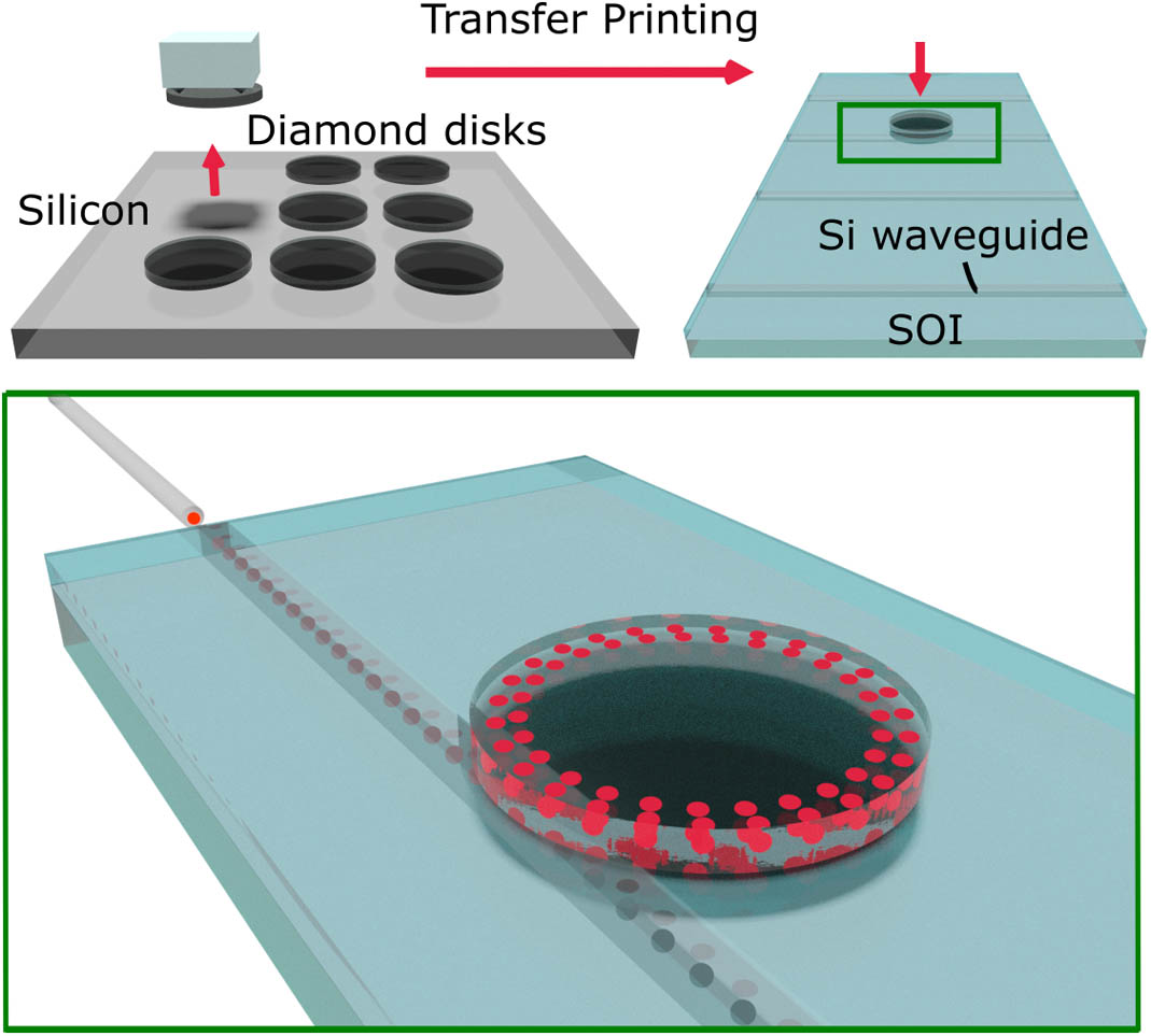
Figure 1.Schematic of a hybrid integration scheme where diamond micro-disk resonators are fabricated separately from a host photonic integrated circuit chip. The fully fabricated diamond resonators are transferred onto the silicon photonic chip using a high-accuracy transfer printing method.
2. METHODS
A. Diamond Membrane Fabrication and Printing
The hybrid integration technique presented in this work is based on a micro-transfer printing method where diamond devices and their host PICs are fabricated separately and assembled using an accurate pick and place tool [16]. In this case the diamond is integrated with a silicon-on-insulator chip, but it is equally applicable to other material systems. In order to ensure high optical mode overlap with the diamond material, disk resonators are used to evanescently couple to the silicon bus waveguide, as shown schematically in Fig. 1. The SCD samples are fabricated using laser dicing and polishing to obtain square pieces with 2 mm side-lengths and a thickness of around 30 μm. The typical wedge gradient of these pieces is of the order of 2.75 μm/mm. In order to isolate the effect of this wedge, monolithic diamond devices can be patterned across the chip, as shown schematically in Fig. 2. The material wedge can be defined along two perpendicular axes, where one, , corresponds to a high rate of change of thickness along that axis, and the other, , corresponds to a low rate of change of thickness with respect to that axis. Devices of the desired thickness can then be selected from the array for integration, for example, selecting a row of devices parallel to . This method allows usage of the whole array through an iterative process of printing target thickness devices, globally etching the full sample until the next set of devices are within tolerance, and repeating the printing.
Sign up for Photonics Research TOC. Get the latest issue of Photonics Research delivered right to you!Sign up now

Figure 2.(a) Schematic of a wedged diamond sample, (b) patterned devices illustrating device thickness selection using an iterative printing and thinning process. (c) Optical micrograph of an array of tessellated squares fabricated on a wedged single crystal diamond sample. The arrows show the axes of low and high material wedge gradient.
Fabrication of the thin-film SCD samples was carried out following our previous work using a lithography and inductively coupled plasma reactive ion etching (ICP-RIE) process [18]. The sample is initially thinned to a few micrometers using an etch. The sample is then transferred onto a silicon carrier chip for patterning. An etch mask is patterned in hydrogen silsequioxane (HSQ) resist using electron beam lithography to ensure smooth sidewall features. Transfer of the pattern into the diamond is achieved using a high platen power ICP etch [18]. After patterning, the hard-mask can be removed using a etch and the membrane can be globally thinned using the etch to the desired thickness, measured using optical profilometry.
To highlight the effect of the material wedge, and the possibility that desired membrane thickness can be selected from an array, a sample was patterned with an array of tessellated squares, separated by 1 μm gaps. Once the free-standing diamond devices are fully etched they can be detached from the silicon carrier substrate using a soft polymer stamp and transferred onto the host substrate. A schematic of the printing process is shown in Fig. 3. Before the physical printing process is carried out, the donor and receiver substrates are spatially referenced in the transfer print tool using registration markers on their surfaces. Once this spatial registration is set, subsequent printing steps are semi-automatic and require tens of seconds to carry out. Once a device is selected, a polydimethylsiloxane (PDMS) stamp is brought into contact with the target membrane, e.g., one square of the tessellated array, and then retracted with a velocity above the critical velocity for object pickup [19]. The membrane adheres to the surface of the stamp and is released from the donor substrate. The object is then positioned over the host substrate and brought into contact. The stamp is removed at a velocity below the critical value, leaving the membrane adhering to the surface. In this work, the smooth surfaces of the diamond membranes and host substrates mean that printing can be achieved without an intermediate adhesion layer. Atomic force microscope (AFM) measurements of the thinned diamond membrane sample exhibit an r.m.s. roughness of . There is no measurable change in r.m.s. roughness after the transfer printing step.
Figure 3.Transfer printing process: (a) resist is spun and (b) patterned on a diamond membrane, (c) the pattern is transferred to the diamond using inductively coupled-plasma reactive ion etching. (d)–(f) A PDMS stamp is aligned with the diamond membrane device, brought into close contact, and retracted to release the membrane. (g)–(i) The membrane is aligned over a host substrate, brought into contact, and released, leaving it transferred on the new substrate.
Eight membranes from the tessellated square array were selected for printing. The first four were selected along the sample axis corresponding to the minimum wedge gradient, , and a further four were selected along the perpendicular axis, corresponding to the maximum wedge gradient, . Their thickness was measured using an AFM. The difference in thickness between each membrane’s highest and lowest corners was used to determine a gradient over the diagonal length, which was found to match the global gradient of the diamond sample measured before patterning. Scanning electron microscope (SEM) images of the printed membranes are presented in Fig. 4(a). Figure 4(b) shows the measured average thickness of the eight printed membranes, showing the ability to select for thickness across a wedged sample. The square with the lowest average thickness was measured with a minimum corner height of , demonstrating the suitability of the printing technique for delicate thin films.
Figure 4.(a) Two 45 deg tilted-view SEM micrographs showing eight membranes from the same original diamond sample, printed onto a silicon substrate. (b) Mean measured thickness for each of the eight membranes demonstrating the possibility of selecting membranes by their thickness, dependent on their original position on the sample.
B. Diamond Micro-Disk Integration
A particular benefit to using transfer printing to assemble micro-photonic devices is that the geometry is not limited to what can be realized in a single planar layer [16,19]. In this case a diamond micro-disk resonator was printed onto a silicon bus waveguide with an upper cladding of silica, giving control over the coupling coefficient between the disk and waveguide using both the vertical and lateral separations of the devices.
To fabricate the SCD micro-disks, the process detailed above for the tessellated square was followed. In this case, the e-beam pattern written into the HSQ resist was an array of micro-disks with a radius of 12.5 μm. The diamond was then etched using ICP-RIE [20]. The material thickness of the selected device was 1.8 μm. Finally, the diamond disk was printed onto a pre-fabricated silicon photonic chip.
The silicon bus waveguide was fabricated on a 220 nm thick silicon-on-insulator material platform, with a width of 500 nm. An upper cladding of HSQ was spin coated onto the chip with a thickness of 250 nm. The silicon waveguide was terminated with an inverse taper and embedded in an SU8 waveguide to allow off-chip coupling to the fiber with low loss.
The micro-disk dimensions allow multiple spatial modes in the cavity that will exhibit different propagation losses and coupling coefficients to the bus waveguide, which is a necessary component for the pump/probe optical cavity tuning presented here. Both the silicon waveguide and diamond micro-disk support TE and TM optical modes. For the upper cladding thickness of 250 nm, the achievable coupling coefficients for the TM mode set were closest to critical coupling and so the remainder of this work will focus on the TM modes. TE modes could be selected by using a different upper cladding thickness. Figure 5 shows calculated mode profiles for the first three radial TM modes of the cavity calculated using a finite difference eigenmode solver. The parameter in Fig. 5 refers to the lateral offset between the edge of the disk resonator and the edge of the silicon waveguide it is being printed onto. By varying this offset, the coupling coefficient between the waveguide and the disk can be controlled. Figure 5(b) shows the variation of the optical power confined to the waveguide area for these modes, showing modification of the ratio of coupling coefficients between them can be achieved by variation of the lateral offset between the disk and waveguide. In previous work we have demonstrated that integrated optical devices can be printed with an absolute positional accuracy in the 100 nm range [16,17]. The lateral mode profiles demonstrated in Fig. 5 exhibit intensity envelopes that vary over the hundreds of nanometers range in the lateral direction, allowing for control of the relative coupling coefficients to the modes by spatial positioning of the disk with respect to the waveguide. In this work the diamond micro-disk was printed with its edge aligned to that of the silicon bus waveguide to allow coupling to a number of spatial modes. An optical microscope image of the printed diamond micro-disk on the silicon waveguide is shown in Fig. 6.
Figure 5.(a) Power distributions of the first three TM whispering gallery modes of a diamond disk resonator with 1.8 μm thickness printed on a silica substrate. (b) Diamond disk mode overlap with the silicon waveguide as a function of lateral offset, , between the disk and waveguide.
Figure 6.Optical microscope image showing a 12.5 μm radius diamond disk integrated with a silicon waveguide using micro-transfer printing.
C. Measurement Setup
The spectral characterizations of the micro-disk resonator and the optical tuning were both realized with the same measurement setup, as shown in Fig. 7. For optical transmission measurements a tunable laser was coupled to the silicon chip using a lensed polarization-maintaining fiber. The output light was coupled to a second lensed fiber and collected with a photodiode and oscilloscope or an optical spectrum analyzer.
Figure 7.Optical measurement setup used for spectral characterization of the integrated micro-disk. The pump laser source, EDFA, and OSA are only used for the pump/probe thermal tuning measurements.
For the thermo-optic tuning measurements, the setup was augmented with a second laser source that was amplified using an erbium-doped fiber amplifier (EDFA) and multiplexed with the low-power tunable laser source through a fiber coupler to a lensed fiber.
3. RESULTS
A. Micro-Disk Transmission Measurements
A transmission spectrum of the diamond micro-disk resonator coupled to the silicon bus waveguide is shown in Fig. 8. As expected from the multiple spatial modes supported by the micro-disk geometry, the spectrum exhibits a large number of resonances.
Figure 8.Normalized transmission spectrum of the hybrid diamond–silicon micro-disk resonator.
The large number of modes measured makes it difficult to identify a particular spatial mode solution. Nevertheless, each resonance can be fitted to an analytic model for an all-pass, whispering gallery resonator to extract values for the coupling coefficient, round-trip propagation loss, and loaded and intrinsic -factors [18]. An average loaded (intrinsic) -factor of () was found, with a representative example of a fitting plotted in Fig. 9(a). There were a number of measured -factors significantly higher than the average, with the largest loaded (intrinsic) -factor resonance plotted in Fig. 9(b) with a value of (). These values are comparable with other diamond resonator devices that have been reported in the literature [4,8,21], showing that the transfer printing process does not induce significant additional optical loss in the resonators. All of the extracted power cross-coupling coefficients and distributed losses across the spectrum are plotted against the loaded -factor in Fig. 10. The resonator distributed loss is the sum of the round-trip propagation loss and coupler excess loss, divided by the cavity round-trip length [22]. As expected, the modes with higher -factors have the lowest losses and cross-coupling coefficients. The correlation between propagation loss and coupling coefficient is likely due to the geometry of the disk coupling region. For larger modal overlap between the disk and waveguide modes, the coupling coefficient will be higher. In addition, this larger modal overlap will correspond to a greater perturbation of the disk mode in the coupler region, leading to increased excess coupler losses.
Figure 9.(a) Measured transmission and fit to analytic all-pass resonator function for a mode around the average loaded -factor of the device. (b) Measured transmission and fitted curve for the highest measured loaded -factor resonance. is the power cross-coupling coefficient, and the loss refers to the distributed propagation loss value of the resonator.
Figure 10.Power cross-coupling coefficients (squares) and distributed losses (circles) as a function of measured loaded -factor.
B. Thermo-Optic Tuning
The micro-assembly of diamond micro-disks onto the insulator provides a mechanism for optically tuning the device resonant wavelengths. Absorption of light results in thermal energy being deposited in the waveguiding material. The resultant increase in temperature induces a material refractive index shift based on the thermo-optic coefficient of index [23]. For devices fabricated in millimeter-size diamond films, the large thermal conductivity [)] of the material and its low thermo-optic coefficient () mean that with typical on-chip power levels in the milliwatt range, resonance tuning is extremely limited. In the hybrid geometry presented here the diamond micro-disk is thermally isolated on the silica cladding of the host chip. Therefore, any thermal energy deposited in the disk can only convect to the surrounding air, conduct through the substrate, or radiate from the surface. Convection and radiation are both low-efficiency processes for diamond devices, the latter due to a small emissivity coefficient of the material. The thermal conductivity of silica is 1.5 W/(m·K), providing good thermal isolation of the diamond micro-disk. Therefore, in this geometry, the combined effect of the optical mode confinement and the thermal isolation of the small diamond resonator, allows for significant temperature increases in the diamond with milliwatt-level optical pumping.
The effect of increasing optical injection power on the resonator refractive index can be measured using the well-known thermo-optic bistability in optical resonators [23]. By sweeping the tunable laser source across a resonance, with increasing wavelength, an asymmetric resonance response is recorded. Figure 11 shows three transmission spectra at different on-chip optical power levels, exhibiting thermo-optic bistability, with increasing redshift as a function of on-chip power.
Figure 11.Transmission spectra of the diamond resonator measured using a continuously swept laser source with on-chip source power as a parameter.
The propagation losses of the optical modes supported in the diamond micro-disk comprise of scattering and absorption components. A resonant mode with high round-trip propagation losses was selected to optically pump the device to maximize absorption and hence thermo-optic tuning of the cavity. The micro-disk can be addressed in a pump/probe setup to decouple the optical signal required for tuning the resonance position and the probe beam used to measure the effective device transmission spectrum. A resonance at a wavelength of 1563 nm, was selected for the pump, and simultaneous measurement of the effective transmission spectrum was taken using the probe beam. The effective resonant shift of the probe measurement is given as a function of the on-chip pump power in the tuning resonance in Fig. 12. Resonant wavelength tuning up to 450 pm was demonstrated for the maximum available pump power of 4.25 mW on-chip. The inset of Fig. 12 shows the probe laser measurement of a single peak that has been shifted. Given a thermo-optic coefficient of for SCD, this translates to a uniform internal temperature of the micro-disk of 46°C. Figure 13 shows a finite element model of the diamond-on-silica-on-silicon cross section at the maximum measured temperature of 46°C, assuming the background environment to be at room temperature. The high thermal resistance of the silica layer that the diamond micro-disk is printed onto allows good confinement of the thermal energy to the diamond material, supporting the thermo-optic tuning effects observed in the measurements. Furthermore, the top surface temperature of the silica layer decreases to ambient levels within 50 μm of the diamond device edge. This strong spatial confinement of the thermal field means that multiple, individual tunable resonators could be integrated together within a fairly compact area.
Figure 12.Probe measured wavelength shift of a resonance centered at for different pump powers injected in the 1563 nm resonance. Inset: probe spectral measurements of a resonant mode at 0 mW and 4.25 mW on-chip pump powers.
Figure 13.Simulation of thermal diffusion in the hybrid diamond-on-silica-on-silicon stack showing high confinement in the printed diamond micro-disk. (a) Schematic of the material stack, (b) thermal simulation close to the micro-disk region.
4. CONCLUSION
In conclusion, micro-fabrication and transfer printing techniques have been developed that enable the heterogeneous integration of monolithic diamond optical devices with non-native substrates. A diamond micro-disk resonator was printed onto a silicon waveguide chip with high alignment precision and exhibiting loaded quality factors of the order of , with a maximum value for one resonance at . Separable thermal tuning and spectral measurement of the resonances were demonstrated, with shifts shown at an on-chip pump level of 4.25 mW. The thermal insulation inherent to the bonding onto silica limits thermal cross talk between devices with spacings of the order of tens of micrometers. Electrically controlled thermal tuning devices are commonly employed in integrated optics [24] and would be straightforward to implement for hybrid diamond on PIC devices. Such localized electronic thermal tuning elements could be used for active and stable tuning of individual diamond devices to align resonances across several devices on a single chip.
Acknowledgment
Acknowledgment. The authors acknowledge the efforts of the staff of the James Watt Nanofabrication Centre at the University of Glasgow.
References
[1] F. Casola, T. Van Der Sar, A. Yacoby. Probing condensed matter physics with magnetometry based on nitrogen-vacancy centres in diamond. Nat. Rev. Mater., 3, 17088(2018).
[2] T. H. Taminiau, J. Cramer, T. van der Sar, V. V. Dobrovitski, R. Hanson. Universal control and error correction in multi-qubit spin registers in diamond. Nat. Nanotechnol., 9, 171-176(2014).
[3] C. E. Bradley, J. Randall, M. H. Abobeih, R. C. Berrevoets, M. J. Degen, M. A. Bakker, M. Markham, D. J. Twitchen, T. H. Taminiau. A 10-qubit solid-state spin register with quantum memory up to one minute(2019).
[4] P. Latawiec, V. Venkataraman, M. J. Burek, B. J. M. Hausmann, I. Bulu, M. Lončar. On-chip diamond Raman laser. Optica, 2, 924-928(2015).
[5] L. Li, T. Schröder, E. H. Chen, M. Walsh, I. Bayn, J. Goldstein, O. Gaathon, M. E. Trusheim, M. Lu, J. Mower, M. Cotlet, M. L. Markham, D. J. Twitchen, D. Englund. Coherent spin control of a nanocavity-enhanced qubit in diamond. Nat. Commun., 6, 6173(2015).
[6] M. J. Burek, J. D. Cohen, S. M. Meenehan, T. Ruelle, S. Meesala, J. Rochman, H. A. Atikian, M. Markham, D. J. Twitchen, M. D. Lukin, O. Painter, M. Lončar. Diamond optomechanical crystals. Optica, 3, 1404-1411(2016).
[7] B. J. M. Hausmann, I. Bulu, V. Venkataraman, P. Deotare, M. Lončar. Diamond nonlinear photonics. Nat. Photonics, 8, 369-374(2014).
[8] B. J. M. Hausmann, B. Shields, Q. Quan, P. Maletinsky, M. McCutcheon, J. T. Choy, T. M. Babinec, A. Kubanek, A. Yacoby, M. D. Lukin, M. Loncar. Integrated diamond networks for quantum nanophotonics. Nano Lett., 12, 1578-1582(2012).
[9] A. H. Piracha, K. Ganesan, D. W. M. Lau, A. Stacey, L. P. McGuinness, S. Tomljenovic-Hanic, S. Prawer. Scalable fabrication of high-quality, ultra-thin single crystal diamond membrane windows. Nanoscale, 8, 6860-6865(2016).
[10] N. Thomas, R. J. Barbour, Y. Song, M. L. Lee, K.-M. C. Fu. Waveguide-integrated single-crystalline GaP resonators on diamond. Opt. Express, 22, 13555-13564(2014).
[11] F. Gao, Z. Huang, B. Feigel, J. Van Erps, H. Thienpont, R. G. Beausoleil, N. Vermeulen. Diamond electron beam lithography, gratings, integrated optics, optical waveguides, proximity effects. J. Lightwave Technol., 34, 5576-5582(2016).
[12] A. A. Kaminskii, V. G. Ralchenko, V. I. Konov. CVD-diamond—a novel χ(3)-nonlinear active crystalline material for SRS generation in very wide spectral range. Laser Phys. Lett., 3, 171-177(2006).
[13] R. P. Mildren. Intrinsic optical properties of diamond. Optical Engineering of Diamond, 1-34(2013).
[14] B. Machielse, S. Bogdanovic, S. Meesala, S. Gauthier, M. J. Burek, G. Joe, M. Chalupnik, Y.-I. Sohn, J. Holzgrafe, R. E. Evans, C. Chia, H. Atikian, M. K. Bhaskar, D. D. Sukavhev, L. Shao, S. Maity, M. D. Lukin, M. Loncar. Quantum interference of electromechanically stabilized emitters in nanophotonic devices(2019).
[15] J. L. Zhang, S. Sun, M. J. Burek, C. Dory, Y.-K. Tzeng, K. A. Fischer, Y. Kelaita, K. G. Lagoudakis, M. Radulaski, Z.-X. Shen, N. A. Melosh, S. Chu, M. Lončar, J. Vučković. Strongly cavity-enhanced spontaneous emission from silicon-vacancy centers in diamond. Nano Lett., 18, 1360-1365(2018).
[16] J. McPhillimy, B. Guilhabert, C. Klitis, M. D. Dawson, M. Sorel, M. J. Strain. High accuracy transfer printing of single-mode membrane silicon photonic devices. Opt. Express, 26, 297-300(2018).
[17] B. Guilhabert, J. McPhillimy, S. May, C. Klitis, M. D. Dawson, M. Sorel, M. J. Strain. Hybrid integration of an evanescently coupled AlGaAs microdisk resonator with a silicon waveguide by nanoscale-accuracy transfer printing. Opt. Lett., 43, 4883-4886(2018).
[18] P. Hill, E. Gu, M. D. Dawson, M. J. Strain. Thin film diamond membranes bonded on-demand with SOI ring resonators. Diam. Relat. Mater., 88, 215-221(2018).
[19] A. Carlson, A. M. Bowen, Y. Huang, R. G. Nuzzo, J. A. Rogers. Transfer printing techniques for materials assembly and micro/nanodevice fabrication. Adv. Mater., 24, 5284-5318(2012).
[20] C. Lee, E. Gu, M. Dawson, I. Friel, G. Scarsbrook. Etching and micro-optics fabrication in diamond using chlorine-based inductively-coupled plasma. Diam. Relat. Mater., 17, 1292-1296(2008).
[21] M. Mitchell, D. P. Lake, P. E. Barclay. Optomechanically amplified wavelength conversion in diamond microcavities. Optica, 6, 832-838(2019).
[22] X. Fengnian, L. Sekaric, Y. A. Vlasov. Mode conversion losses in SOI photonic wire based racetrack resonators. Opt. Express, 14, 3872-3886(2006).
[23] V. R. Almeida, M. Lipson. Optical bistability on a silicon chip. Opt. Lett., 29, 2387-2389(2004).
[24] A. H. Atabaki, A. A. Eftekhar, S. Yegnanarayanan, A. Adibi. Sub-100-nanosecond thermal reconfiguration of silicon photonic devices. Opt. Express, 21, 18312-18323(2013).


