Electromagnetic wave absorbers operating in the microwave, THz, infrared, visible, and ultraviolet bands have become a prevalent research topic. The typical electromagnetic wave absorber is a vertically stacked multilayer structure based on a metal-dielectric-metal (MIM) structure. The optical characteristics of metal, semiconductor, and new materials can be utilized to optimize the absorption of incoming electromagnetic waves. Absorption mechanisms such as local plasmon resonance, magnetic polariton resonance, surface plasma resonance, Fabry-Perot cavity resonance, and guide mode resonance can be used to realize ideal absorption effects. Infrared absorbers with efficient, broadband, and tunable properties are urgently required in optical sensors, photothermal energy converters, imaging, and infrared stealth cloaks. However, in practical applications, achieving a broadband response in the infrared band is difficult. Most proposed infrared absorbers are limited to the near-infrared (NIR) range and are untunable. Therefore, an ultra-broadband tunable absorber operating from near-infrared to far-infrared is proposed, and its absorption mechanism is analyzed.
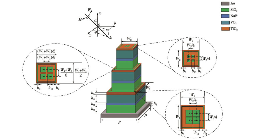
An infrared broadband absorber is designed based on the phase material VO2, metalloids, and high-temperature resistance materials NaF and TiO2. First, owing to the unique properties of the materials, the material properties are set based on the role and characteristics of different materials. The ports at the upper and lower ends along the z-direction are set separately, the port type is periodic, and the two ports are set to open and close,respectively. Second, the domains, boundaries, and edges of the different materials in the structure are meshed in detail. Parametric sweeping is then performed according to the study band, and the electric field distribution and the magnetic field are obtained. Finally, the optimal result is obtained through repeated calculations by adjusting the structural geometric parameters, angle of incidence, and polarization angles of the transverse electric (TE) and transverse magnetic (TM) waves.
After several simulations, the optimization parameters are obtained: the cell period is 7 μm, the width of the bottom composite layer is 5.8 μm, the width of the top composite layer is 3.4 μm, the thickness of Au is 0.9 μm, the thickness of SiO2 layer is 0.9 μm, the thickness of NaF layer is 0.1 μm, the thickness of VO2 layer is 1.0 μm (the conductivity is set as 2×10¹⁵ S/m), and the thickness of TiO2 layer is 0.3 μm. The ratio between the edge length of each group of top square holes and the edge length of each group of composite layers is 0.05, the distance between the outside of the SiO2 square ring and the outside of the composite layer is 0.1 μm, and the width of the square ring is 0.1 μm. Figure 3 shows that the ultra-wideband absorption in the wavelength range of 12-52 μm, and the polarization insensitivity can be achieved using this absorber. Figure 4 shows that when the TM wave is incident, the angle of incidence increases to 55° in the range of 12-52 μm, and the absorptivity can reach approximately 80%. When the TE wave is incident, the angle of incidence increases to 55° in the range of 20-45 μm, and the absorptivity reaches approximately 80%. Figure 5 shows that the absorption mechanism of the absorber is surface plasma resonance. The physical mechanism of absorption can also be better understood from the impedance-matching plot (Fig. 6). The structural parameters have a substantial impact on the absorption performance. Figure 7 shows the absorptivity curves for different structural parameters and the corresponding magnetic field distribution maps to determine the optimal parameters. Figure 8 shows the absorption spectrum changes with VO2 conductivity. Finally, Fig. 9 compares the absorption effect of the SiO2 pattern in the uppermost layer of each multilayer structure. We determine that, when the SiO2 pattern is observed, the absorption bandwidth is wide and the absorption effect is high. Table 1 compares the main performance indicators of the infrared absorber designed for this study and the existing infrared absorber to further demonstrate the superiority of the proposed structure.
A truncated infrared broadband absorber is designed based on the phase material VO2, metalloids, and high-temperature resistance materials NaF and TiO2. Using the finite element method, the dependences of the absorptivity on the type of incident wave, angle of incidence, azimuth angle, incident wavelength, and geometric parameters are further analyzed. The results demonstrate that the absorption mechanism of the infrared broadband absorber is the surface plasma resonance effect. When the TM wave is incident, the angle of incidence increases to 55° in the range of 12-52 μm, and the absorptivity can reach approximately 80%. When the TE wave is incident, the angle of incidence increases to 55° in the range of 20-45 μm, and the absorptivity reaches approximately 80%. When TM or TE waves are incident vertically, three absorption peaks are formed around 14 μm, 24 μm, and 40 μm, which are named p1, p2, and p3, respectively. At 21-25 μm and 35-43 μm, the absorptivity reaches 99.8%; the absorptivity is more than 90% at 12-51 μm, the average absorptivity of the broadband absorber reaches 96.4%, and the relative bandwidth reaches 124%. Further, the absorptivity is polarization insensitive. The infrared absorber designed in this study is expected to be widely used in infrared sensing, detection, energy harvesting, and energy conversion.