
Zhenzhen Li, Weiqiang Liu, Ruixia Wu, Yunhui Li, Jing Shao. Influence of Host Material on Performances of Green Organic Light Emitting Diodes[J]. Laser & Optoelectronics Progress, 2019, 56(22): 222302
- Laser & Optoelectronics Progress
- Vol. 56, Issue 22, 222302 (2019)
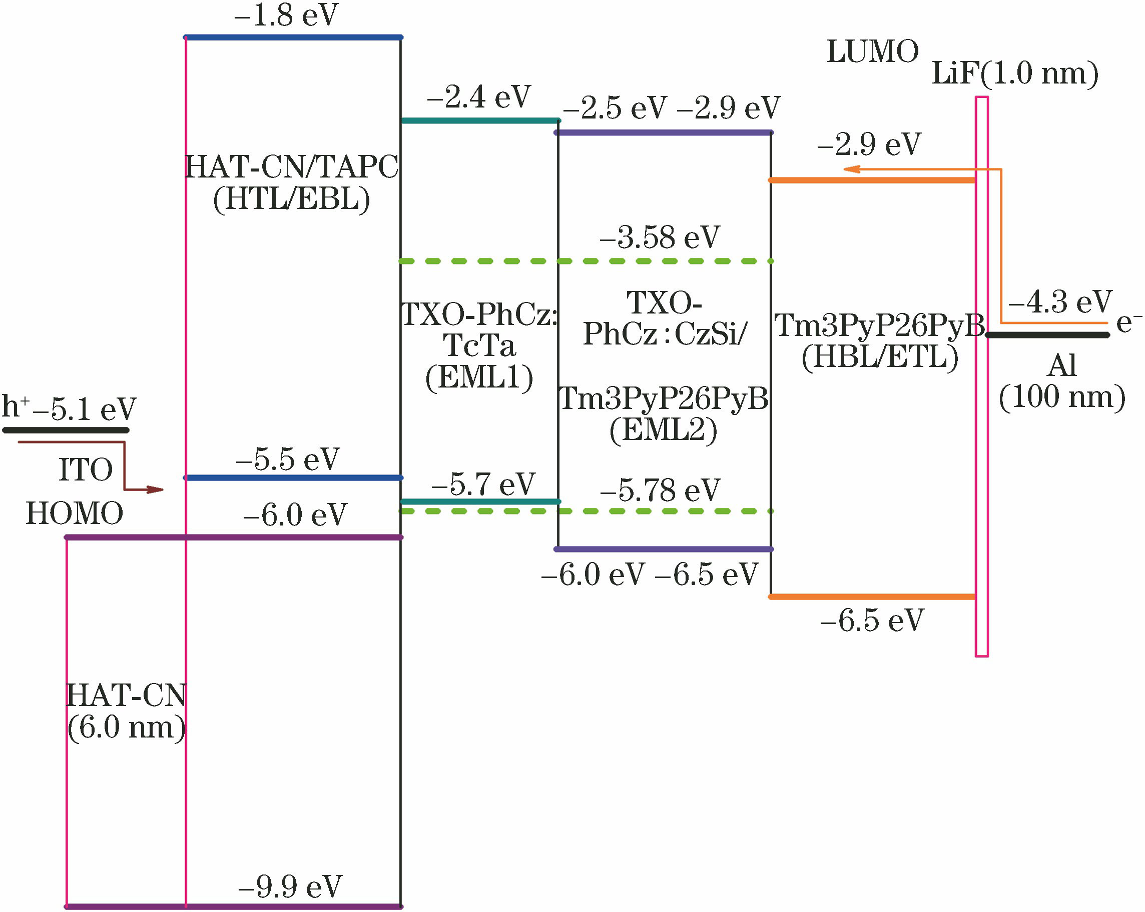
Fig. 1. Energy-level structure of device (symbols of ‘h+’ and ‘e-’ represent hole and electron, respectively)
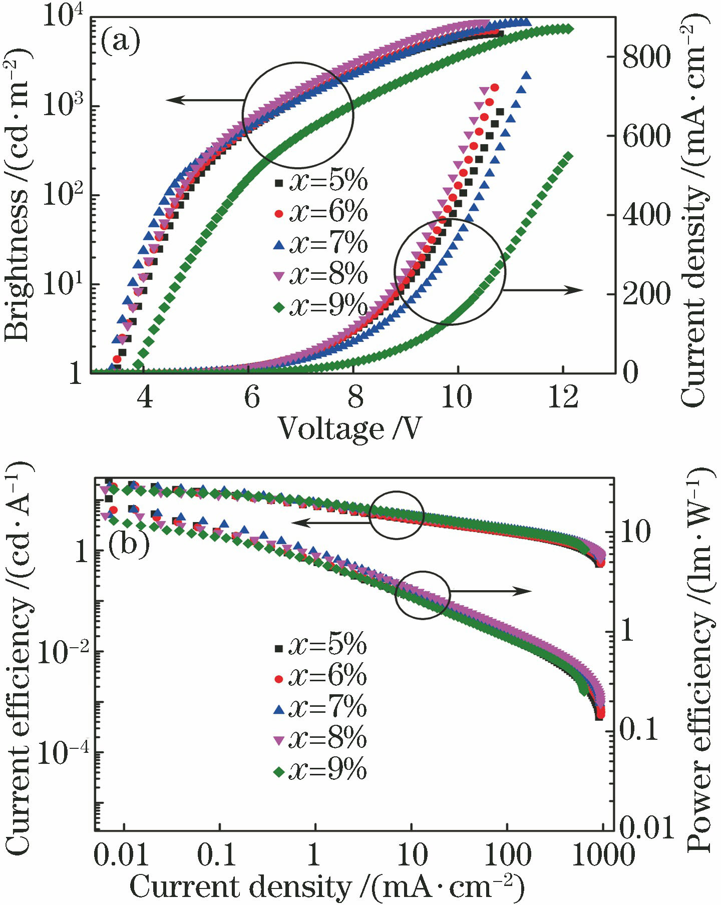
Fig. 2. Performances of TXO-PhCz doped CzSi single-emitting layer devices with different concentrations. (a) Relationship among voltage, brightness, and current density; (b) relationship among current density, current efficiency, and power efficiency
Fig. 3. Performances of TXO-PhCz doped Tm3PyP26PyB single-emitting layer devices with different concentrations. (a) Relationship among voltage, brightness, and current density; (b) relationship among current density, current efficiency, and power efficiency
Fig. 4. Diagrams of carrier injection and transmission of single-emitting layer devices. (a) Diagram of carrier injection and transmission of TXO-PhCz doped CzSi single-emitting layer device; (b) diagram of carrier injection and transmission of TXO-PhCz doped Tm3PyP26PyB single-emitting layer device
Fig. 5. Spectra of TXO-PhCz doped CzSi single-emitting layer devices with different concentrations
Fig. 6. Spectra of TXO-PhCz doped Tm3PyP26PyB single-emitting layer devices with different concentrations
Fig. 7. Performances of TXO-PhCz doped CzSi double-emitting layer devices with different concentrations. (a) Relationship among voltage, brightness, and current density; (b) relationship among current density, current efficiency, and power efficiency
Fig. 8. Performances of TXO-PhCz doped Tm3PyP26PyB double-emitting layer devices with different concentrations. (a) Relationship among voltage, brightness, and current density; (b) relationship among current density, current efficiency, and power efficiency
Fig. 9. Carrier diagrams of double-emitting layer. (a) Carrier diagram of double-emitting layer using TcTa and CzSi as host materials; (b) carrier diagram of double-emitting layer using TcTa and Tm3PyP26PyB as host materials

Set citation alerts for the article
Please enter your email address
© Copyright 2018-2021 | Chinese Laser Press. All Rights Reserved 沪ICP备15018463号-20