Due to its strong piezoelectric effect and photo-elastic property, lithium niobate is widely used for acousto-optical applications. However, conventional bulk lithium niobate waveguide devices exhibit a large footprint and limited light–sound interaction resulting from the weak guiding of light. Here, we report the first acousto-optical modulators with surface acoustic wave generation, phononic cavity, and low-loss photonic waveguide devices monolithically integrated on a 500 nm thick film of lithium niobate on an insulator. Modulation efficiency was optimized by properly arranging the propagation directions of surface acoustic waves and optical guided modes. The effective photo-elastic coefficient extracted by comparing the first and third harmonic modulation signals from an on-chip Mach–Zehnder interferometer indicates the excellent acousto-optical properties of lithium niobate are preserved in the thin film implementation. Such material property finding is of crucial importance in designing various types of acousto-optical devices. Much stronger amplitude modulation was achieved in a high Q () optical resonator due to the higher optical sensitivity. Our results pave the path for developing novel acousto-optical devices using thin film lithium niobate.
1. INTRODUCTION
The interaction between light and mechanical waves has long been investigated and widely utilized to synthesize various acousto-optical (AO) devices [1]. One category of AO devices, including modulators, deflectors, tunable filters, correlators, and other signal processors, is based on the photo-elastic effect, which describes the change in index of refraction in a material induced by the applied strain [2]. These devices are extensively applied in optical network and signal processing applications. Moreover, the coherent coupling between optical and mechanical modes mediated by electromagnetic radiation pressure is exploited in stimulated Brillouin scattering/amplification and cavity optomechanical systems that may trigger and expedite the development of ultrasensitive force sensors and quantum information processing technology [3–5].
With the development of piezoelectric transducer technology and the rapid growth of integrated optics, great attention has been drawn to thin film AO devices. A surface acoustic wave (SAW), whose energy is mainly confined near the surface, can be effectively generated by well-established interdigital transducers (IDTs) formed on the surface of piezoelectric substrates [6]. When SAWs are used to interact with integrated photonic waveguides, the AO device footprint can be scaled down to an on-chip implementation and, similarly, the coupling between the acoustic and optical fields is significantly enhanced as the SAW and waveguide modes are co-propagating and interacting near the surface and hence boosting their overlap [7].
Lithium niobate (LN) is well known for its diversified properties like nonlinear-optical, electro-optical, pyroelectric, piezoelectric, and photo-elastic effects [8], allowing realization of a wide range of devices such as high-speed modulators, frequency converters, entangled photon sources, and microelectromechanical systems (MEMS) [9–12]. For AO applications, LN is an ideal candidate for implementing AO devices because of its remarkable piezoelectric and photo-elastic effects. These properties make it possible to simultaneously assemble SAW generation (usually excited by IDTs) and AO functionalities on a single chip without the need to heterogeneously integrate other functional materials [13]. However, traditional bulk LN waveguides, routinely formed by means of titanium indiffusion and proton exchange [14,15], suffer from a large size due to the weak light confinement. For example, the typical mode size of titanium indiffused waveguides is dozens of square micrometers (μ), and the bend radius is on the order of centimeters [14]. Thanks to the breakthrough of lithium niobate–on–insulator (LNOI) technology (single-crystal thin film lithium niobate bonded on a low-index buffer layer), optical modes can shrink to submicrometer dimensions and thus allow the achievement of compact devices and higher integration density as well as dramatically enhanced light–matter interaction [16]. In Ref. [17], Jiang et al. reported experiments on cavity optomechanics realized on LNOI. Recently, our group showed that the AO effect can be applied for rotation sensing in an AO gyroscope [18].
Sign up for Photonics Research TOC. Get the latest issue of Photonics Research delivered right to you!Sign up now
Here we present, to the best of our knowledge, the first AO modulator (AOM) fabricated on LNOI. The photo-elastic coefficient of this platform is extracted for the first time. The well-preserved AO properties in LNOI show promising prospects for implementing a variety of AO devices with high AO coupling strength and compact size [19]. Harnessing the AO properties of LNOI, AO modulation is also showcased in a high-Q optical resonator, which, given the strong optical field enhancement, exhibits up to 10 times stronger modulation than the Mach–Zehnder interferometer (MZI)-type modulator and outperforms state-of-the-art AO modulators fabricated in gallium arsenide (GaAs).
Differently from the high-bandwidth electro-optical modulators demonstrated in LNOI [9] that are used in broadband communication systems, the MHz AO modulators demonstrated herein have a wealth of different and impactful applications including inertial sensing (which favors low frequency) [18], holographic storage/imaging [20], and light beam steering [21]. In addition, the strong regulation of optical signal in a high-Q resonator showcased in this work has enormous potential for on-chip stimulated Brillouin scattering (SBS) applications [22] and broadband frequency comb generation.
2. DESIGN
A. Efficient AO Interactions
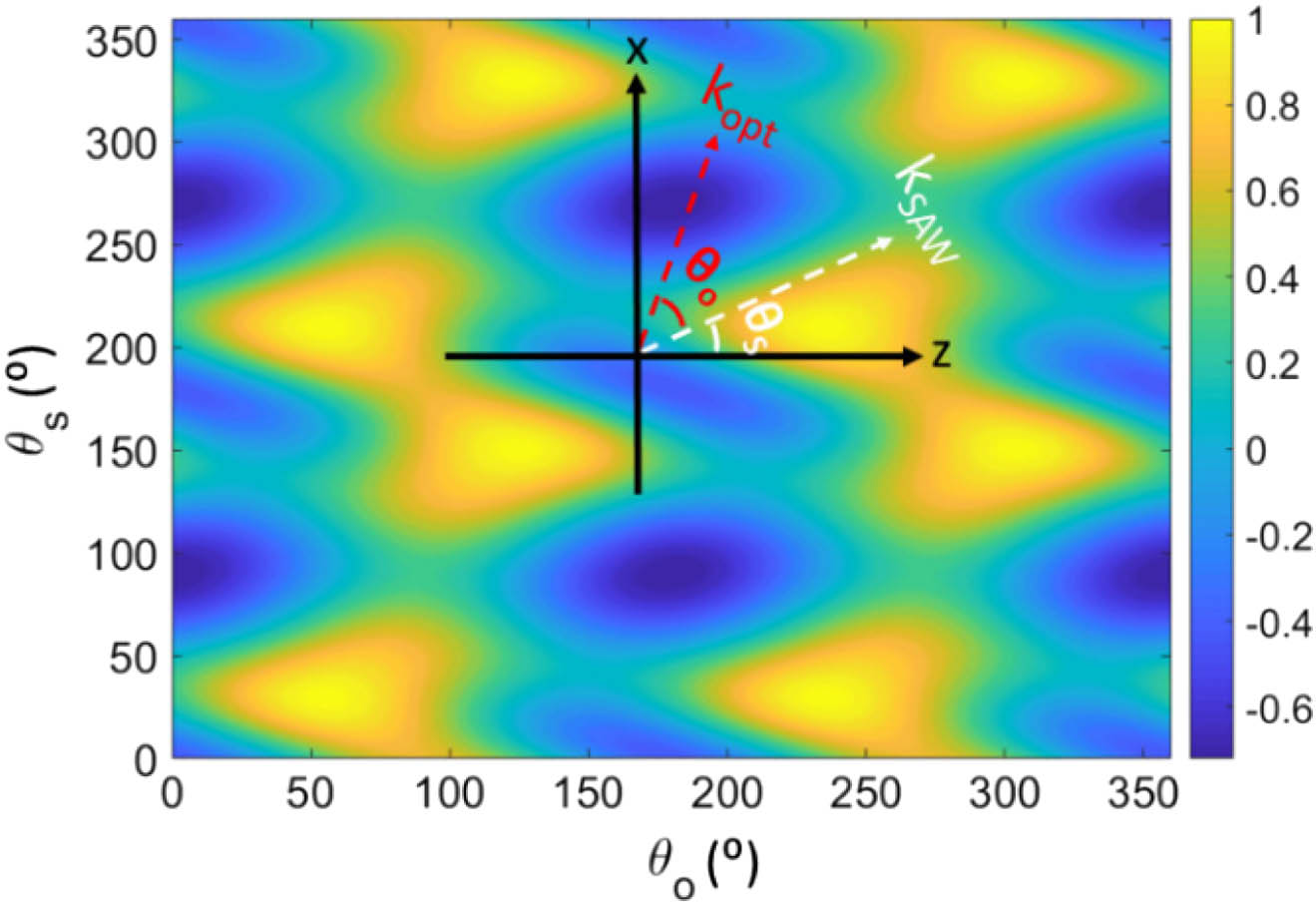
Y-cut LN was selected to harness high electromechanical coupling [23]. The SAW and optical mode were guided in the plane. To maximize the modulation efficiency, we calculated the refractive index change (normalized to its maximum) as a function of the SAW and optical wave propagation directions ( and ) as shown in Fig. 1. is the angle of with respect to the crystal axis, and is the angle between and . The index changes periodically with and , and the maximum index change—or equivalently, the highest modulation efficiency—happens when or , where and are integers. The detailed derivation procedure for calculating index change can be found in Appendix B.
Figure 1.Dependence of refractive index change (normalized to its maximum) on and .
For the purpose of simplifying device layout (i.e., avoiding the use of curved electrodes for the excitation of SAW in LN), attaining greater device packing, and most importantly ensuring uniform index change along the waveguide, it is desirable to make orthogonal to the waveguide . For these reasons, should be set to 90°, and hence the corresponding that maximizes the index change should be selected to be either 45° or 135°.
B. AO Modulators
Figures 2(a)–2(c) show the schematic layouts of the two types of AO modulators that were implemented in this work: the MZI-type AO modulator and the racetrack (RT)-resonator-type AO modulator (referred to as MZI-type AOM and resonator-type AOM in the rest of the paper). The chip stack structure is thin film lithium niobate (TFLN) on a buried oxide (BOX) layer on LN substrate. We adopted split IDTs for launching the SAW to reduce reflection losses [24]. In this proof-of-concept demonstration, the pitch size of the split IDTs (being equal to the wavelength of SAW, ) was selected to be 30 μm so that the minimum feature size was μ and could be easily defined by a mask aligner lithography system. The eigenfrequency of the Rayleigh SAW generated by this IDT was 117 MHz as obtained by the COMSOL finite element method simulation. The corresponding strain profile is given in Appendix A. If particular applications require higher frequencies, the SAW device can be readily extended to operate at gigahertz (GHz) by virtue of electron-beam lithography patterning. Two reflectors with the same pitch size as the IDT were placed on the two sides of the IDT to form a phononic cavity. This acoustic cavity ensures that the SAW becomes a standing wave, and its amplitude is enhanced by the mechanical quality factor () of the device [24]. The number of metal electrodes forming each reflector is 400, which is sufficiently large to ensure a high for the SAW cavity. Both IDT and reflectors are made of Pt, since Pt has high acoustic mechanical reflectivity. The aperture lengths of the IDTs for the MZI-type and resonator-type AOMs are 1.2 mm and 2.4 mm, respectively.
Figure 2.(a) Cross-section rendering of the AO modulator. Note that dimensions are not to scale and the actual SAW of this implementation propagates more deeply in the substrate. (b) and (c) Schematic layouts of MZI- and resonator-type AOMs. Light (green arrows) is coupled to/from the chip by grating couplers. An SAW is launched by the split IDT, and its amplitude is enhanced in the cavity formed by the reflectors (acting as acoustic mirrors). Drawings are conceptual renderings and not to scale. The acoustic cavity (black dashed line) is much larger than the MZI and RT resonators ( for MZI and for the RT).
Light was coupled to/from the devices by grating couplers (GCs), which were selected to ensure future dense integration of photonic devices [25]. When the SAW propagates through the arms/straight segments of the MZI/resonator, the photo-elastic effect changes the phase of the optical signal and hence modulates the output light. In order to maximize the modulation efficiency, the arm closer to the IDT was placed at the maximum amplitude of the strain (, the distance between the last finger of the IDT and the waveguide), and in the MZI-type AOM, the distance between the two arms () was set to be at an odd multiple of to enable push-pull operation. In the resonator-type AOM, the separation between the two straight waveguide arms of the RT was set to be an even multiple of to maximize the accumulated optical phase change. A multi-mode interference 3 dB coupler is used to combine the two arms of the MZI.
For the MZI-type AOM, the first three harmonics of the modulated power can be derived as follows: where is the th order of a Bessel function of the first kind and is a parameter that lumps together the losses of the device and signal conversions in the measurement setup. is the initial phase difference between the two arms of the MZI arising from fabrication errors. is the optical phase change induced by the SAW. is proportional to the square root of the electrical power applied to the IDTs: where depends on the intrinsic properties of the material and device (see Appendix C for its full expression and derivation).
For the resonator-type AOM, the modulation powers of the first and second modulation harmonics are given as (see Appendix C for details) where is the transmission spectrum and is the single-pass phase shift in the RT resonators. As is closely related to the resonator attenuation coefficient and coupling coefficient , the dependence of the optical sensitivity ( and ) on and is plotted in Fig. 3, in which was selected to maximize the sensitivity for each combination of and . In the experiment, we bias the resonator at a particular by changing the lased wavelength. A high-Q (large value of and ) resonator and critical coupling () are desirable to achieve high modulation efficiency. The waveguide width (W) and gap are set to be 1.5 μm and 300 nm, respectively, in the experiment to allow the resonator to roughly operate under the critical coupling condition based on the characterization results of the resonators with various combinations of these two parameters.
Figure 3.Dependence of the (a) first and (b) second derivative of transmission with respect to on and .
The devices were fabricated on a Y-cut LNOI having a 500 nm thick TFLN on top of a BOX layer on LN substrate. The thickness of the BOX was chosen to be 1.5 μm, so as to achieve a good trade-off between the waveguide loss and SAW electromechanical coupling. In fact, as a thicker BOX layer lowers the waveguide loss, it deleteriously impacts the SAW devices [26]. First, the IDT and reflectors made of 600 nm thick Pt were patterned by photolithography and lift-off. Then 350 nm thick Au with 50 nm Cr (seed layer) was patterned via a second lithography and lift-off step. The Au layer is used to form the pads for probing and wire bonding. Finally, the photonic components were patterned by electron-beam lithography and Ar plasma etching in an inductively coupled plasma–reactive ion etching (ICP-RIE) tool, followed by Radio Corporation of America (RCA) cleaning () to remove any residues and byproducts after dry etching [26,27]. The microscope and scanning electron microscope (SEM) images of the fabricated devices are shown in Fig. 4.
Figure 4.Microscope pictures of (a) MZI- and (b) resonator-type AOMs. (c) SEM image of the photonic waveguide (tilted view). (d) SEM image of the IDT region (top view).
The LNOI sample was placed in a pin grid array (PGA) package, and the IDT pads were wire bonded to a printed circuit board to facilitate measurement. The setup for the AOM characterization is shown in Fig. 5(a). Light from a tunable laser (SANTEC TSL510) was launched into the waveguide through a polarization-maintaining fiber. The IDT was driven by an RF signal generator (E4433B ESG-D Series). The outcoupled modulated light was amplified by an erbium-doped fiber amplifier (EDFA, OEQuest EDFA-PA-M) before it was fed into a photodetector (Newport 1414). Finally, the output of the photodetector was displayed with a spectrum analyzer (SA, Keysight Technologies N9000B CXA), and the peak values of the different harmonics in the frequency domain were recorded. The total insertion loss of the photonic circuit is measured to be 20 dB, which is mainly attributed to the grating coupler loss.
Figure 5.(a) Measurement setup for characterizing AOM. PC, polarization controller; RF SG, RF signal generator; DUT, device under test; EDFA, erbium-doped fiber amplifier; PD, photodetector; SA, spectrum analyzer. (b) Detected modulation power (normalized to the maximum) of the first harmonic when the frequency of RF SG is swept. The Q factor of the acoustic cavity is 1800. (c) Measured (triangle) and theoretical (solid line) first, second, and third harmonic signals as functions of the square root of the driving power from the RF SG when the frequency is fixed at 111.725 MHz. All are normalized to the maximum first harmonic modulation power of . (d) Ratio of first to third harmonic signals (log scale) as a function of the square root of the input power from RF SG. and are extracted to be 0.053 and 0.073 rad/√mW, respectively.
The frequency of the RF signal was swept to identify the maximum modulation intensity for the first harmonic. This maximum is located at 111.725 MHz [Fig. 5(b)], which, as expected, corresponds to the peak of the acoustic resonance. The bandwidth is 62 kHz corresponding to a Q factor of 1800. measured at resonant frequency is , indicating that the coupling efficiency is 42%. The response time (modulation speed) of the AOMs in this work is limited by the relatively low frequency of the SAW (determined by the design parameters, i.e., pitch size of 30 μm), and its modulation rate is defined by the narrow bandwidth of the SAW. The work in Ref. [7] reported the GaAs AOM operating at about 500 MHz. We can readily extend our AOMs to higher frequencies by reducing the IDT pitch [24]. Figure 5(c) shows that the measured modulation power of the first, second, and third modulation harmonics recorded from the SA increases with the square root of the input power from the RF SG. The amplitude of the mechanical strain is directly proportional to the square root of the applied electrical power, so the plot offers a direct correlation of the output harmonic power with the generated strain.
To precisely evaluate photo-elastic coefficients, we compared the first and third modulation harmonics to get rid of the influence of the measurement setup () and the mismatch between the two arms () on the modulation power [see Eq. (1)]. Their ratio () only depends on the SAW-induced phase change. As shown in Fig. 5(d), the experimental data fits well with the theory when is set to be 0.053, which falls in the normal range of its theoretical value (0.035–0.087). The theoretical value range is calculated based on different combinations of the related coefficients, such as the primary photo-elastic and electro-optical coefficients [see Eq. (B4) in Appendix B]. Note that these coefficients reported in Ref. [8] are measured at 633 nm, and hence discrepancies are expected since the MZI-type AOM in this work operates at 1550 nm. In addition, the we are reporting here also lumps in the AO overlap factor [see Eq. (C4) in Appendix C], effectively making its value smaller than the intrinsic photo-elastic coefficients. Based on the experimental data and these considerations, we can conclude that the AO properties of LN are well preserved in LNOI.
To the best of our knowledge, this is the first time that the photo-elastic coefficients for TFLN have been experimentally measured and extracted. This contribution is of paramount importance in designing and implementing AO modulators in LNOI for a variety of applications such as AO tunable filters [28], light beam scanning/steering (e.g., lidar) [21], holographic storage [20], and cavity optomechanical systems [17].
By taking the value of extracted above, the phase change imposed by the acoustic wave can be calculated at any power or voltage applied to the IDT. , the coefficient that relates the phase change as a function of the square root of the applied power, is for the MZI-type AOM. This value is comparable to state-of-the-art AOMs fabricated in other interesting AO materials such as GaAs [29]. The LNOI demonstration of this work actually attains the same performance of Ref. [29] if scaled by the optical wavelengths at which the two devices are operated. One advantage of the GaAs implantation is that because of its high refractive index (), a similar value of can be attained over a shorter AO interaction length. On the other hand, LN exhibits a high electromechanical coupling coefficient ( for Y-cut [23]), which is much higher than that of GaAs, and hence it dramatically simplifies the design of SAW devices and facilitates matching to RF driving sources in a much smaller form factor.
An alternative way to evaluate the performance of the LNOI AOM is to compare it to an electro-optic modulator (EOM). It is possible to define an equivalent (a figure of merit defined as the product of the voltage required to induce a phase shift of in the modulator and the interaction length ) for the AOM. This figure of merit is evaluated to be 5 V·cm for the specific MZI AOM we have demonstrated herein. Interestingly, this value is comparable to that of electro-optical modulators fabricated in LNOI [30].
2. Racetrack Resonator AO Modulator
A high-Q optical resonator can be used to enhance the modulation strength of an AOM. A similar approach was reported in an AlN platform [31]. Herein, and differently from Ref. [31], we use an LNOI RT resonator placed inside an acoustic cavity. The transmission spectrum of the fabricated RT resonator shown in Fig. 6(a) illustrates a free spectral range (FSR) of 157 pm. Hence, a group index () of 2.32 can be calculated as [32], where is the optical wavelength and is the perimeter of the resonator. The value of 2.32 compares well with the theoretical value of for the fundamental TE-like mode whose profile is shown in the inset of Fig. 6(b). This confirms that the fundamental TE-like mode is coupled into the waveguide by the GCs as expected. By fine-tuning the wavelength around one of the resonant peaks around 1601.53 nm and fitting the measured data, we extracted a loaded () and intrinsic () of 266,000 and 532,000, respectively [see Fig. 6(b)]. The high extinction ratio () indicates that the resonator is critically coupled. As discussed in the section of AO modulator design (Fig. 3), the high Q and critical coupling facilitate high modulation efficiency. The average waveguide loss was evaluated to be as low as 0.7 dB/cm by dividing the intrinsic loss of RT (0.5 dB, from ) by its total length. It is important to note that this is the overall loss of the RT and includes not only propagation losses but also bend losses clearly present in the RT.
Figure 6.(a) Transmission of the RT resonator for a broad wavelength range. (b) Measured (blue circle) and Lorentzian fit (red) transmission of one of the resonances around 1601.53 nm. Inset: mode profile of the fundamental TE-like mode.
Figure 7(a) shows the modulation power of the first and second modulation harmonics as a function of the square root of the driving power from the RF SG. It was observed that the resonant linewidth would broaden when the acoustic power increased as shown in the inset of Fig. 7(a). This phenomenon is due to nonlinearity arising from strong modulation signals, as it is also observed in EO-modulated RT resonators [33]. To fit the experimental data by theory, the variation of the optical sensitivity [ and in Eq. (2)] in the whole driving power range is extrapolated (see Appendix D for details). A good overlap between the fitting curves and the measured data was obtained as shown in Fig. 7(a).
Figure 7.(a) Measured (triangle) and theoretical (solid line) first and seconnd harmonic signals as functions of the square root of the driving power from RF SG. All are normalized to the maximum first harmonic modulation power of . The reason for the modulated power being lower in the resonator-type AOM than in the MZI-type AOM is that the EDFA is not used in the measurement of the RT resonator. Inset: transmissions of RT resonator when is off (blue), 8 dBm (green), and 15 dBm (red). (b) Measured (green circle) and theoretical (green dash) first harmonic signal as the laser wavelength is swept around the resonance of the RT. The maximum modulation is located at the highest slope of the transmission curve. (c) The gain of the resonator-type AOM relative to MZI-type AOM as a function of the square root of the driving power.
The laser wavelength (at a fixed power of 15 dBm from the RF SG) was also swept to record the modulation response as a function of the wavelength detuning around resonance. Figure 7(b) shows that the response follows the square of the derivative of the Lorentzian transmission given by Eq. (2) for the resonator with (0.032 W), further confirming that it is the SAW that is modulating the optical phase in the resonator.
By taking into account the differences in the measurement setup and the different insertion loss of the on-chip devices and different interaction lengths, it is possible to directly compare the efficiency of the modulation process in the MZI-type and resonator-type AOMs. Such comparison is shown in Fig. 7(c), where the gain, defined as the ratio of the modulation power in the resonator-type AOM to that in the MZI-type AOM, is plotted as a function of the driving power. The gain drops as modulation power increases. This is again due to the widening of the linewidth of the RT resonator response as the driving electrical power increases. Thanks to the high optical sensitivity of the resonator, about 10 dB gain can be achieved at the lower power end, effectively making one of the most efficient AOMs ever demonstrated in a compact form factor.
4. CONCLUSION
In conclusion, we demonstrated the first AO modulators fabricated on lithium niobate thin film. The IDT, acoustic cavity, and low-loss photonic waveguides are fully integrated on chip. The effective photo-elastic coefficient was extracted to be 0.053 in the MZI-type AOM, which agrees well with the theoretical value and indicates that the elasto-optic properties of the bulk material are well preserved in the thin film implementation. The outstanding AO properties combined with the strong guiding of light can trigger the development of the next generation of AO devices implemented in LNOI with unprecedented performance and smaller form factors when compared with bulk LN AO devices. The AO modulation is further demonstrated using a high-Q RT resonator, which exhibits stronger modulation than that of MZI-type AOM and any other integrated platform (e.g., thin film GaAs). The strong AO interaction/coupling in a high-Q system is very promising for novel applications such as Brillouin scattering/amplification, cavity optomechanics, and frequency comb generations.
Acknowledgment
Acknowledgment. We thank S. Hiramatsu and Dr. Yuji Hori from NGK Insulators, Ltd. for providing the LNOI wafers. Any opinions, findings, and conclusions or recommendations expressed in this publication are those of the authors and do not necessarily reflect the views of DARPA.
APPENDIX A: MODELING OF A RAYLEIGH SAW
The eigenmode of the SAW device was simulated by finite element methods in COMSOL Multiphysics. A periodic boundary condition was applied to the left and right edges of the unit cell with a length of one acoustic wavelength. , the SAW wave vector, is directed along the axis, which is rotated by from the crystal axis as discussed in the main text. Figures 8(a) and 8(b) show the displacement profiles in the () and () directions, respectively. The strain distribution in the LN thin film (in the and directions), which is the gradient of the displacement, is shown in Figs. 8(c) and 8(d) with abbreviated subscription notation (, ). The shear strain is weak compared with and and not shown.
Figure 8.Displacement components (a) and (b) . The scale bar is 5 µm. Strain field and in the (c) and (d) direction. Both and are normalized to the maximum of . The LN thin film surface is at .
APPENDIX B: REFRACTIVE INDEX CHANGE THROUGH THE AO EFFECT
LN is a uniaxial crystal. The index ellipsoid of LN is shown in Fig. 9 with its principal axes coinciding with the crystalline axes (). Assuming a Y-cut substrate, the SAW and optical wave co-propagate in the plane. We assume an angle of with respect to the crystalline axis and an angle between and the optical wave vector (). In the new reference ( is along ), the ellipsoid equation becomes where and are the ordinary and extraordinary refractive index of LN, respectively. When the strain is applied onto the material, the ellipsoid equation becomes where the index change is related to strain by the effective photo-elastic coefficient tensor [19] The effective photo-elastic tensor is comprised of direct and indirect contributions as follows [19]: where , , , and are the primary photo-elastic coefficient, piezoelectric coefficient, electro-optic coefficient, and dielectric constant, respectively. is the unit vector along . The second term (indirect contribution) arises from the fact that the strain induces an electric field in the material through the piezoelectric effect, and, in turn, causes index change through the electro-optical effect. For a material like LN, which possesses very strong piezoelectric and electro-optic effects, such an indirect term cannot be ignored.
Figure 9.Refractive index ellipsoid of LN. are crystalline principle coordinates. is in the plane and rotates by angle with respect to . is the relative angle between and .
Since a Rayleigh SAW is launched and is perpendicular to (), only and strain fields , , and need to be considered in Eq. (B3) as follows: Moving boundary effect was also considered [34] but found to be negligible for the contribution to the phase change compared to that from the photo-elastic effect. The factor “2” is attributed to the push-pull structure of the MZI-type AOM and interaction length of in resonator-type AOM. is the electric field of the fundamental TE-like mode. can be expressed as the product of its amplitude and profile, . Since is weak, Eq. (C2) can be simplified to The minus sign is due to the fact that the phase difference between and is . is the ratio of to that can be obtained from Fig. 8. is the resonant angular frequency of SAW, and is the overlap between the strain ( or ) and optical field, which is defined as The energy density of the acoustic wave is Since the thickness of TFLN is much smaller than the SAW wavelength, we can regard to be constant in the direction in the TFLN. Integrating over the whole cavity, the energy in TFLN solely contributed by is (, of IDT, approximately equal to the AO interaction length), which accounts for about 5% () of the total energy () in the SAW cavity according to the simulated strain field distribution. can also be expressed as a function of the measurable acoustic and the power P injected into the cavity as is evaluated by measuring the reflection of the , where is the source power from the signal generator. Then we get the final expression of the amplitude of as follows: Inserting Eq. (C8) into Eq. (C3), we obtain
MZI-Type AOM
The transmission of an MZI followed by a 3 dB coupler is where is the phase difference between the two arms arising from mismatches in fabrication of the arms or errors in the making of the 3 dB coupler. Using the Jacobi–Anger expansion, Eq. (C10) can be decomposed to the following different modulation harmonics: where is the Bessel function of the first kind. Considering the laser power (), the insertion loss of the on-chip device () and the conversion gain from EDFA () and PD (), we obtain the modulation power detected by spectrum analyzer for these harmonics as follows: The square in Eq. (C13) is attributed to the fact that the output voltage of the PD is squared to obtain the power displayed by the spectrum analyzer, which has internal impedance, .
Resonator-Type AOM
The transmission of a bus waveguide side-coupled to an RT resonator is [35] where is the single-pass phase shift in the resonator with total length of and is the phase change induced by the SAW device. and are the attenuation coefficient and the self-coupling coefficient, respectively. Equation (C14) can be expressed through a Taylor series evaluated at as Hence, we get the amplitude of the first and second harmonics as Again, considering the signal conversion between the instruments, the power displayed on the spectrum analyzer is To get the highest modulation efficiency, for example, of the first modulation harmonic, one need to bias (achieved by fine-tuning the laser wavelength) at the highest slope of the transmission spectrum.
APPENDIX D: DEPENDENCE OF OPTICAL SENSITIVITY ON THE SAW POWER
To precisely fit the measured data by theory in Fig. 7(a), one needs to know the variation of the optical sensitivity, and , in the whole power range. Figure 11 shows the extracted resonator attenuation coefficient and coupling coefficient at three electrical power levels. decreases with the square root of the power from RF SG, while almost remains unchanged. The value of was extrapolated through the whole power range by fitting the three points [black line in Fig. 11(a)], and the corresponding first (second) derivative of with respect to is shown as the green (orange) line in Fig. 11(b). The fitted values are used to match the fitted curves to the experimental results shown in Fig. 7(a) of the main text.
Figure 11.(a) Extracted and from the transmission spectra of resonator at three power levels ( is off, 8 dBm, and 15 dBm). The black line is the linear fitting of . (b) The first (green) and second (orange) derivative of with respect to , respectively.