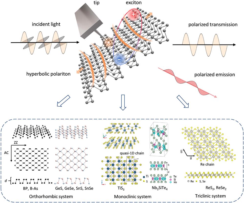
Fig. 1. Light–matter interaction and atomic structures of anisotropic 2D semiconductors.
Fig. 2. Interband absorption of anisotropic 2D materials. (a) Absorption spectra of 1L, 2L BP (left)
[34], bulk-like GeS (middle)
[64], and 1L–3L
(right)
[37]. The photoreflectance of GeS is also shown in the middle panel. (b) Polarization dependence of interband absorption of BP (left)
[35], GeS (middle)
[64], and
(right)
[37]. 0° corresponds to AC direction for BP and GeS, but for
, it corresponds to
axis (Re chain). (c) Illustration of interband transitions at
point of BP. (d) Photocurrent spectra of thin
(
) (left)
[99] and absorption spectra of thin
(
) (right)
[102]. (e) Layer-dependent bandgap and interband transitions. Left panel: first three transition energies of BP and
versus layer number. Data are taken from Refs. [
35,
37,
38]. Right panel: bandgap ranges of various anisotropic materials (BP,
, MX,
, NST) with thickness from bulk to monolayer. Data are taken from Refs. [
35,
37,
38,
60,
97,
102].
Fig. 3. Photoluminescence spectra of anisotropic 2D materials. (a) PL of BP. Left two panels: PL of monolayer
[34] and multi-layer (thickness from 4.5 to 46 nm) at 77 K
[116]. Middle right panel: PL peak positions in atomically thin BP reported by several groups
[34,49,103–110" target="_self" style="display: inline;">–110]. Right panel: linear polarization dependence of PL emission in monolayer BP
[34]. Emission intensity follows
function, where
is the angle with respect to AC direction. (b) Illustration of PL process. (c) PL of multilayer GeS (
)
[63]. Top panel: polarization dependent PL spectra of GeS, where “A” (“∥
a”) corresponds to excitation (detection) polarized along AC direction. Bottom panel: PL emission intensity versus detection polarization angle. (d) PL of
[85]. Top panel: PL spectra with different detection polarization angles of few-layer
(
) at 4 K (one at 300 K shown in inset). At low temperature, five PL peaks can be discerned. Bottom panel: first two PL peak intensities versus detection polarization angle, where 0° corresponds to
axis (Re chain). (e) PL of
[123]. Top panel: PL spectra under different detection polarization angles of multi-layer
(
) at low temperature (20 K). Spectra are divided into two regions, where D denotes defect states PL, and X denotes intrinsic interband PL. Bottom panel: emission intensities of D and X versus detection polarization angle
, where
axis is parallel to the quasi-1D Ti-chain.
Fig. 4. Excitons in anisotropic 2D materials. (a) Schematic illustration of excitons. Top panel: illustration of the optical absorption of an ideal 2D semiconductor
[126]. Series of exciton states (
,
,
, etc.) below the quasiparticle bandgap are shown. Bottom panel: real-space illustration of excitons in an anisotropic 2D material (left) and a typical exciton wave function calculated for monolayer BP (right)
[44]. (b) Layer-dependent excitons in few-layer BP. Top left panel: typical extinction spectrum of BP (tri-layer) with high crystal quality on PDMS substrate
[141].
state can be clearly discerned as indicated by the red arrow. Top right panel: layer dependence of
and
transition energies and the quasiparticle bandgap
in 2L–6L BP
[141]. Bottom left panel: layer dependence of absorption due to excitons in 2L–7L BP, where
is the universal absorption of monolayer graphene
[129]. Bottom right panel: absorption near the corresponding band edge due to the continuum part of each interband transition in 2L–7L BP
[129]. The continuum absorption is nearly independent of the material thickness. (c) Calculated optical absorption with/without excitonic effect in monolayer GeS (left) and GeSe (right)
[36].
X corresponds to AC direction. (d) Excitonic absorption in
. Left panel: transmission and calculated absorption spectra of monolayer and bulk
[38]. Near band edge, two prominent peaks can be discerned, which are superpositions of four excitonic resonances labeled as
. Right panel: differential reflectance spectra of multi-layer
(
) under different polarized incident lights (with respect to the
axis, as shown in inset)
[144]. Four excitonic absorption peaks labeled as
can be discerned. (e) Excitons in other anisotropic 2D system. Top left panel: schematic illustration of band structure, exciton A, and sideband A′ in bulk
. Top right panel: experimental PL spectrum and calculated absorption spectrum of
with/without exciton–phonon interactions
[146]. Bottom left panel: illustration of exciton–phonon coupling via
phonon mode modulated ligand field transition in
. Bottom right panel: linear dichroism spectrum of a thin bulk
flake at 5 K
[147].
Fig. 5. Nonlinear optics of anisotropic 2D materials. (a) Saturable absorption. Left panel: schematic illustration of saturable absorption. Middle left panel: power-dependent transmittance with incident polarization angle changing from
axis (AC) to
axis (ZZ) in the exfoliated thick BP flake (thickness
)
[155]. Middle right panel: typical open aperture Z-scan curves of SnSe nanosheet dispersion under 230 fs excitation pulses with wavelength of 1030 nm
[160]. Right panel: polarization-dependent absorption of
(thickness
) at low incident power of
and at high power of
(left top), and polarization-dependent ratio of absorption between that under 1.55 and
incident power (left bottom)
[156]. The right one is a schematic of excited-state absorption in
. (b) Third harmonic generation (THG). Left panel: schematic illustration of THG. Middle panel: typical THG spectrum of multilayer BP flake (thickness
) under excitation wavelength of
(left), and polar plot of polarization dependence of THG from BP flake (thickness
) on glass substrate (right), where red and purple arrows indicate AC and ZZ directions, respectively
[163]. Right panel: THG power of BP in transmission (orange) and in reflection (blue) versus thickness. The resonance THG occurred at thickness
as indicated by pink area
[161]. (c) Second harmonic generation (SHG). Left panel: schematic illustration of SHG. Middle left panel: SHG spectra from bilayer
and monolayer
pumped by a laser at 1558 nm. Insets are polar plots of SHG parallel components from bilayer
and monolayer
[165]. Middle right panel: SHG intensity in 1L–8 L
[165]. Right panel: SHG of SnS film (thickness
) at different excitation wavelengths
[166].
Fig. 6. Band structure engineering of anisotropic 2D materials. (a) Electrical field effect on BP. Top left panel: schematic illustration of the BN-sandwiched device with graphene as top gate and Si substrate as bottom gate for applying vertical electrical field
[173]. Top right panel: PL spectra of the 20-layer BP under different displacement fields (
) ranging from 0 to 0.48 V/nm
[173]. Middle left panel: bandgap of the 20-layer BP extracted from PL spectra (dots) and first-principles calculations (curve) versus
[173]. Bottom left panel: schematic illustration (top) and ARPES spectra (bottom) of BP band structure under different surface K-dopings
[174]. Bottom right panel: absorption spectrum of a 9L BP before and after chemical doping through
vapor (top) and enlarged view of the hybrid peaks between
and
(bottom)
[35]. (b) Strain and pressure effect. Left panel: schematic illustration of application of uniaxial strain (top)
[177], biaxial strain (middle)
[181], and pressure (bottom)
[188]. Right top panel: normalized PL spectra of multilayer BP (
) under zero strain, compressive strain (
along the zigzag direction), and tensile strain (
along the zigzag direction)
[177]. Right middle panel: linear shift rates of interband transition (
,
, and
) peaks induced by biaxial strain versus layer number in 2L–10L BP
[181]. Dots are experimental data, and solid curves are fittings through the tight-binding model. Right bottom panel: relative change of the optical bandgap of BP versus pressure
[188]. Dots are experimental data, and solid curves are the fittings. (c) Alloying and intercalation. Top panel: crystal structure of
[195] (left) and absorption spectra of
with different constituent ratios
x from 0 to 0.83 (right)
[190]. Middle panel: schematic illustration of intercalation process by CTAB to form the BP superlattice (left) and high resolution TEM images of BP before and after intercalation (right)
[195]. After intercalation, in-plane lattice parameter negligibly changes but interlayer distance has nearly two-fold enlargement. Bottom panel: electrochemical gate current as a function of the applied electrochemical potential (left), and PL signal observed at different stages of intercalation (right)
[195]. (d) Homo and heterostructures based on BP. Top panel: schematic illustration of the crystal structure and band diagram of few-layer BP and monolayer
heterostructure (left), and PL spectra of different thickness BP and
heterostructures at 80 K
[200]. Bottom panel: illustration of BN encapsulated 1L and 2L twisted BP homostructure and TEM image of a 5.7° twisted 1L/2L BP structure (left), scale bar 2 nm. PL spectra of the 1L, 2L BP and 19° twisted BP homostructure (right)
[203]. An emerging moiré optical transition at 0.83 eV is observed in twisted homostructure.
Fig. 7. Schematic of polariton topological transitions. (a) IFCs in the momentum space and the
component of the electric field in real space of surface plasmons supported by BP in purely anisotropic, quasi-circular, and hyperbolic regimes
[231]. (b), (c), (d) Hyperbolic regimes induced by anisotropic phonons, plasmons, and excitons for phonon
[232], plasmon
[39], and exciton polaritons
[110], respectively.
Fig. 8. Methods to probe polaritons. (a) Schematic to stimulate polaritons in the far field. Due to the momentum mismatch, light in free space is unable to excite polaritons directly. Additional momentum can be supplied by Kretschmann or Otto configuration, fabricating gratings by the side of material or resonant nanostructures
[238]. (b) Resonant modes of LSPR in graphene nanoribbons with different widths
[15]. [(c)-a] Schematic illustration of the near-field technique to image propagating plasmon polaritons at the surface of graphene on
with s-SNOM. [(c)-b, c, d, e] Near-field amplitudes of interference pattern close to graphene edges (blue dashed lines), defects (green dashed lines and dot), and at the boundary between single and bilayer graphene (white dashed line)
[208]. (d) Diagram of STEM-EELS experimental setup. (e) Typical EEL spectrum of
in aloof geometry. Blue: sharp ZLP with an FWHM of about 8 meV after spectrum normalization. Green: energy loss area. Yellow: fitted background. Red: extracted five major vibrational signals
[232].
Fig. 9. In-plane hyperbolic PhPs in
. (a) Lattice structure of
. Inset shows an octahedron of one Mo atom and six O atoms
[232]. (b) Images of near-field amplitudes of an
slab (250 nm thick) at 990 and
incident laser frequencies. (c) Nano-FTIR spectra along the [100] (left panel) and [001] (right panel) axes. (d) Near-field amplitudes in real space and IFCs in momentum space (corresponding Fourier transform) of the elliptical and hyperbolic PhPs in
nanodisks
[40]. (e) HAADF image of an
nanoribbon (about 100 nm thick) in STEM. The inset shows an electron diffraction pattern obtained near the ribbon edge. (f) EELS maps taken in the yellow dashed box in (e)
[232].
Fig. 10. Hyperbolic characteristics in other natural materials. (a), (b) Lattice structures of
[243] and
[244] respectively. (c) Real part (continuous lines) and imaginary part (dashed lines) of the permittivity along the principal [100], [001], and [010] axes in
. [(d)-a] Dispersion of PhPs in
[244]. Dots are the extracted experimental data from the near-field interference pattern. Black curves represent the calculated
propagating modes. The pseudo color maps are calculated as the reflection coefficient by the transfer-matrix method. [(d)-b, d, f] IFCs of
calculated for three characteristic frequencies (8.35, 7.5, 6.8 THz) within the different RBs, respectively. [(d)-c, e, g] 3D representation of simulated field distributions
at the same frequencies as [(d)-b, d, f], respectively, for a 224 nm thick
slab between air and Si substrate.
Fig. 11. In-plane hyperbolic plasmon polaritons in
. (a) Lattice structure of orthorhombic
. (b) Schematic of the extinction spectrum measurement. (c) Optical microscope image of exfoliated
thin film (60 nm thick) on
substrate. (d) FIR extinction spectra at 10 K of the specimen in (c). (e) Temperature dependence of the in-plane effective mass ratio calculated by the fitted Drude weight. (f) MIR extinction spectra of
bare film along different crystal axes at 10 K. (g) LSPR of
microdisk on
substrate along different crystal axes at 10 K. (h) Dispersion relation of plasmons along different crystal axes in
measured in rectangle arrays. (i) IFCs of plasmons in
at different frequencies
[39].
Fig. 12. Hyperbolic plasmon polaritons theoretically predicted in BP. (a)–(f) Conductivity tensor of BP versus real in-plane wave vector due to nonlocality. (g)–(j) Nonlocal effect on the IFCs of plasmons calculated at
, chemical potential
for (i), (j) and
,
for (g), (h). (k), (l) Spontaneous emission rate of a
-oriented point source as a function of its distance to BP films and graphene sheets, considering local and nonlocal effects
[231]. (m), (n) Calculated real and imaginary parts of conductivity of BP along armchair (
) and zigzag (
) directions for different carrier densities, respectively. (o) IFCs of plasmons with conductivity given in (m) and (n), with
,
for the blue line,
,
for the red line, and
,
for the green line
[210].
Fig. 13. Evidence for the existence of hyperbolic exciton polaritons in few-layer BP films
[264]. (a) Optical contrast image of monolayer BP. (b) Reflection spectra of monolayer BP with polarization along AC and ZZ directions. (c) Imaginary parts of optical conductivities of monolayer BP along AC and ZZ directions extracted from the reflection spectra in (b). Real and imaginary parts of optical conductivities along AC direction of (d) monolayer BP and (e) 2L–4L BP. (f) Layer dependence of the hyperbolic regime of few-layer BP. Shaded areas in all panels indicate hyperbolic regimes.
Fig. 14. Twist angle induced topological transitions of phonon polaritons
[225]. (a) Schematic of twisted bilayer structure of
films. (b) Phase diagram of the polariton topology as a function of rotation angle and polariton frequency. Green dashed line indicates the boundary of topological transitions.
is the number of anti-crossing points of the iso-frequency contour dispersion of each isolated layer. [(c)-a] Schematic of propogating polaritons launched by a tip. [(c)-b, c, d] Optical images of
bilayer structures with different twist angles. [(c)-e, f, g, h] Maps of the near-field intensity near the point defects. [(c)-e] Measured bare
film in the right black dashed square of [(c)-d]. [(c)-f, g, h] Results of the twisted bilayers in [(c)-b, c, d]. [(c)-i, j, k, l] Dispersion curves of polaritons by Fourier transform of the measured results in [(c)-e, f, g, h].
Fig. 15. Topology engineering of phonon polaritons by leveraging the substrate. (a) Right panels: schematics of propagation of phonon polaritons launched by a dipole source of
films on different substrates:
and 4H-SiC. Left panels: IFCs of polaritons at
of
films on substrates corresponding to the right panels
[228]. (b) Topological transition of phonon polaritons of
on 4H-SiC substrates with different polariton frequencies. Top panels: schematic illustration of the topology change of hyperbolic dispersion at different frequencies. Middle panels: evolution of experimentally measured near-field amplitude launched by antennas as a function of the frequency. Bottom panels: left parts show the simulated IFCs through the Fourier transformation of simulated near-field distributions, and right parts show the analytical IFCs for the fundamental mode
[228]. (c) Analytical hyperbolic IFCs of phonon polaritons of
on top of air (red line) or SiC (blue line) substrate. The arrows indicate the wave vectors at different tilted angles
. At some angles, wave vectors are allowed for one dispersion (solid arrow) while forbidden for the other (dashed arrow). [(d)-a] Schematic of SiC cavities with different shapes. [(d)-b, c, d] Numerically simulated field distribution of polaritons of
films suspended on SiC substrates with different air cavities at
. [(d)-e] Schematic of the excitation of directional propagating polaritons of
films at the air–SiC interface. [(d)-f, g, h] Polariton excitation of
at the interface of SiC and air with different rotation angles
[229].
Fig. 16. Intercalation effect. (a) (left) Lattice structure illustration of
and intercalated
. (a) (middle and right) Polariton dispersion from nano-FTIR line spectral scan along [100] and [001] directions for
(middle) and
(right), respectively
[243]. (b) (left) Schematic of tip launched propagating phonon polaritons in
in-plane heterostructure. (b) (right) Optical images and near-field amplitude images of
,
, and
after dehydrogenation. Scale bar is 5 µm
[278]. (c) (left) Setup for the metal intercalation of
. (c) (right) Azimuthal angular acoustic phonon dispersion for the original
and
after Cu, Co, and Sn intercalation
[279].
Fig. 17. Active tuning of hyperbolic phonon polaritons in
heterostructures. (a) (left) Schematic of the
heterostructure under s-SNOM measurement. Upper inset shows the optical image of the heterostructure. Lower inset illustrates the charge transfer process of graphene via
. [(a) (right)-a, b] Maps of near-field amplitude of hybrid polaritons in
heterostructures under different graphene doping levels. [(a) (right)-c] Line profiles of hybrid polaritons along [100] and [001] directions at different doping levels of graphene at
. [(a) (right)-d] Line profiles of hybrid polaritons along [100] and [001] directions at different frequencies
[226]. (b) (left) Schematic of
heterostructure on the
substrate. (b) (right) IFCs extracted from near-field measurements of hybrid polaritons of
on
substrates at different graphene doping levels. (c) (left) Schematic of
heterostructure on Au substrate. (c) (right) Near-field experimental measurement of propagating hybrid polaritons exhibiting partial focusing
[284].
Fig. 18. Polarization engineering by natural hyperbolic 2D surfaces. (a) (left) Schematic of the polarizer based on natural hyperbolic films (
and
) on Si substrate. (a) (middle and right) Transmission and extinction ratio of polarizers based on
(middle) and
(right) films with different thicknesses
[285]. (b) (left) Schematic for the MIM structure for extrinsic chirality, where
and
represent the oblique angle of incident light and tilted angle in the
plane, respectively. (b) (middle) CD dissymmetry factor
in Ag based MIM as a function of wavelength and oblique angle
. The parameters for the MIM structure are
,
,
, and
. (b) (right) Absorption spectra of an Au based multilayer MIM structure, with the top Au film nanostructured to a cube. The cube thickness is optimized for 780 nm
[290]. (c) (left) Schematic diagram for a twisted bilayer structure of
. (c) (middle) Transmission spectra of LCP and RCP light and the related CD in twisted bilayer structure as a function of rotation angle. (c) (right) Transmission spectra as a function of the incident angle. Thicknesses of bottom and top slabs are 0.6 and 2.72 µm respectively. Wavelength of incident light is 14.4 µm
[292]. (d) (left) Schematic illustration of the asymmetric transmission process that supports the asymmetric transmission of circularly polarized light. (d) (right) Real parts of dielectric constant of bismuth (top). Circular asymmetric transmission
of bismuth as a function of the in-plane tilted angle
and wavelength
(bottom). The thickness of the bismuth slab is 4.5 µm, and the angle of incidence is 60°
[293].
Fig. 19. Polariton propagation manipulation. [(a)-a] Topographic image of Au nanoantennas with rod-like trapezoid shaped
crystal. The separation
is 320 nm. Phonon polaritons excited from the edges of the antennas interfere at the spot marked by a red circle. [(a)-b, d] Images of near-field amplitude for the rod-like trapezoidal nanoantennas in [(a)-a] by experiment and simulation. [(a)-c] Profiles of the field intensity along the arrows in [(a)-b, d]
[218]. [(b)-a, d, g] Three different heterostructures for the excitation of APhPs by dipoles: isotropic heterostructure [(b)-a],
heterostructure [(b)-d], and
heterostructure [(b)-g]. [(b)-b, e, h] Corresponding near-field electric intensity simulation above the Au surface at
. Insets show the cross-section view in the
xz plane. [(b)-c, f, i] Corresponding IFCs by Fourier transform
[220]. [(c)-a, b] Illustration of negative reflection for hyperbolic phonon polaritons in momentum and real space. Here, Poynting vectors
Si and
Sr are on the same side. [(c)-c, d] Illustration of negative backreflection for hyperbolic phonon polaritons in momentum and real space. Here,
Si =
Sr. [(d)-a, b] Experimental result of the near-field electric intensity distribution of hyperbolic phonon polaritons backreflected by mirror of
with different tilted angles. [(d)-c] Poynting vectors and wave vectors of incident and reflected HPhPs in IFCs for the illustration of backreflection
[297].
Fig. 20. Unidirectional propagation. (a) Schematic illustration of tip launched unidirectional propagation of phonon polaritons via diffraction from blazed grating in the surface of
crystal. Mirror symmetry is possibly broken by rotating the in-plane direction of the grating angle. [(b)-a, b, c] Schematic of diffraction of normal, bidirectional, and unidirectional diffraction of phonon polaritons by grating with different shapes and in-plane rotation angles.
indicates the diffraction state. + implies the wave vector direction, and
U indicates the propagation of polaritons on the upside of the grating. [(b)-d, e, f] The hot spots are the Fourier transform of the calculated real space electric field distribution of phonon polaritons excited by corresponding gratings on left side. The yellow lines show the IFC of hyperbolic polaritons in
. (c) (top) Scanning electron microscopy images of circular-hole and blazed gratings fabricated on
flakes with different rotation angles. (c) (middle) Images of near-field amplitude of first-order diffraction of phonon polaritons excited by gratings in top panels. Bidirectional propagation is observed in gratings with circular holes, and unidirectional propagation is observed in blazed gratings. (c) (bottom) Fourier transform of the images in the middle panels
[304].
Fig. 21. Spontaneous emission enhancement and biosensing of natural hyperbolic surfaces. (a) (left) Schematic of
slab. (a) (right) Evaluation of the modulation factor of
as a function of rotation along different axes
[305]. (b) Spontaneous emission enhancement of air/graphene/
/Si heterostructure with different doping levels of graphene. Dipoles polarized along different axes are placed above the heterostructure
[282]. (c) (left) Schematic of molecular sensing enhancement in the monolayer
nanogap/Au heterostructure using nano-FTIR technique. (c) (middle) Dispersion curves of phonon polaritons in different
structures. Black curve: 5 nm thick freestanding
layer. Red curve:
5 nm/air gap 0.6 nm/Au. Blue curve: freestanding
monolayer. Green curve: monolayer
gap 0.6 nm/Au. (c) (right) Normalized electric field spectra of APhPs in
nanoribbon/air gap 0.6 nm/Au (red dashed line). The spectrum of APhPs coupling with single molecules is shown in red solid curve. The spectrum amplified by 50 times for the bare molecule is plotted as blue solid curve
[306].
Fig. 22. Management of thermal radiation and heat transfer. (a) (left) Schematic diagram of arrays of indefinite square cavities made of aligned films of single-wall carbon nanotubes. A spacer is between the cavities and substrates. The square lattice has edge lengths of
and
along and perpendicular to the tube axis. (a) (middle) Measured relative emissivity of square cavity arrays with different edge lengths (unit in µm). They have nearly identical emission peaks at
. (a) (right) IFC at
calculated from the measured dielectric constant of single-wall carbon nanotubes. The points are extracted from the results in (a) (middle)
[311]. (b) (left) Schematic of two twisted hyperbolic systems for investigating the near-field heat transfer. The twisted bilayer system consists of two identical graphene nanoribbons with ribbon width of
and air gap of
. The top and bottom twisted systems are treated as an emitter and receiver, respectively, with
. (b) (right) Spectra of RHF between the twisted system with different rotation angles
[312]. (c) (left) HTC of monolayer
under different tensile and compressive strains. Two monolayer sheets are separated by a gap
of 10 nm here. (c) (right) HTC spectra under different tensile strains. The vertical dashed lines indicate the energy for topological transition between elliptic and hyperbolic regimes
[313].
Material Type | Material | Thickness | Substrate | Binding Energy/eV | Exciton Radius/Å | Polarization | Notes | BP | BP | 1L | w/o | [41,42,125,126] | 8.2(x), 2.3(y)[133] | AC(x) | Multi-interband | | | | w | 0.3–0.45[102,106,108], 0.9[104] | | | | | | Bulk | / | | | | | MX (M = Ge, Sn; X = S, Se) | GeS | 1L | w/o | [34,128,129] | 6.7(x), 4.5(y)[34] | AC(x) | Multi-valley exciton | | | | w | [129] | | | | | | Bulk | / | <0.1 | | | | | GeSe | 1L | w/o | [34,130,129] | 21.2(x), 15.4(y)[34] | | | | | | w | [129] | | | | | | Bulk | / | <0.1 | | | | | SnS | 1L | w/o | [34,128] | 15.1(x), 15.1(y)[34] | | | | | Bulk | / | <0.1 | | | | | SnSe | 1L | w/o | [34,130] | 27.3(x), 25(y)[34] | | | | | Bulk | / | <0.1 | | | | (X = S, Se) | | 1L | w/o | [70,131] | | | | | | | w | | | from Re chain | | | | Bulk | / | [70,119] | 10[119] | Re chain | | | | 1L | w/o | [36,70,131] | 7.5[36] | | | | | | w | 0.52[132] | | from Re chain | | | | Bulk | / | [36,70] | 9.6[36] | Re chain | | Quasi-1D materials | | 1L | w/o | [96,97] | 7.8(x), 7.4(y)[133] | Out-of-plane | | | | Bulk | | [97,134] | | | | | | Bulk | | 0.14[135] | | Perpendicular to quasi-1D electron chain | 1D electrons, 2D holes | 2D magnets | | >2L | w | | | | Exciton-magnon coupling | | CrSBr | 1L | w/o | [136] | | Parallel to quasi-1D electronic chain | Strong quasi-1D electronic structure |
|
Table 1. Comparison of the Lowest Exciton in Anisotropic 2D Materials.