• Photonics Research
  • Vol. 10, Issue 8, 1900 (2022)
Jie Xu1, Changjun Min1、3、*, Yuquan Zhang1、4、*, Jielei Ni1, Gengwei Cao1, Qianyi Wei1, Jianjun Yang2, and Xiaocong Yuan1、5、*
Author Affiliations
  • 1Nanophotonics Research Center, Shenzhen Key Laboratory of Micro-Scale Optical Information Technology & Institute of Microscale Optoelectronics, Shenzhen University, Shenzhen 518060, China
  • 2State Key Laboratory of Applied Optics, Changchun Institute of Optics, Fine Mechanics and Physics, Chinese Academy of Sciences, Changchun 130033, China
  • 3e-mail: cjmin@szu.edu.cn
  • 4e-mail: yqzhang@szu.edu.cn
  • 5e-mail: xcyuan@szu.edu.cn
  • show less
    DOI: 10.1364/PRJ.458613 Cite this Article Set citation alerts
    Jie Xu, Changjun Min, Yuquan Zhang, Jielei Ni, Gengwei Cao, Qianyi Wei, Jianjun Yang, Xiaocong Yuan. Imaging ultrafast evolution of subwavelength-sized topography using single-probe structured light microscopy[J]. Photonics Research, 2022, 10(8): 1900 Copy Citation Text show less
    Schematic of the SPSLM, where red and violet indicate pump light (at 800 nm) and probe light (at 400 nm), respectively. (a) Diagram of ultrafast pulses on Si wafer. (b) Optical path of SPSLM: BBO, barium boron oxide; DM1, DM2, dichroic mirrors; L1–L6, lenses; R1–R5, reflectors; BS1, BS2, beam splitters; DMD, digital mirror device; CCD, charge-coupled device; MO, microscope objective (100×, apochromatic, NA=0.9).
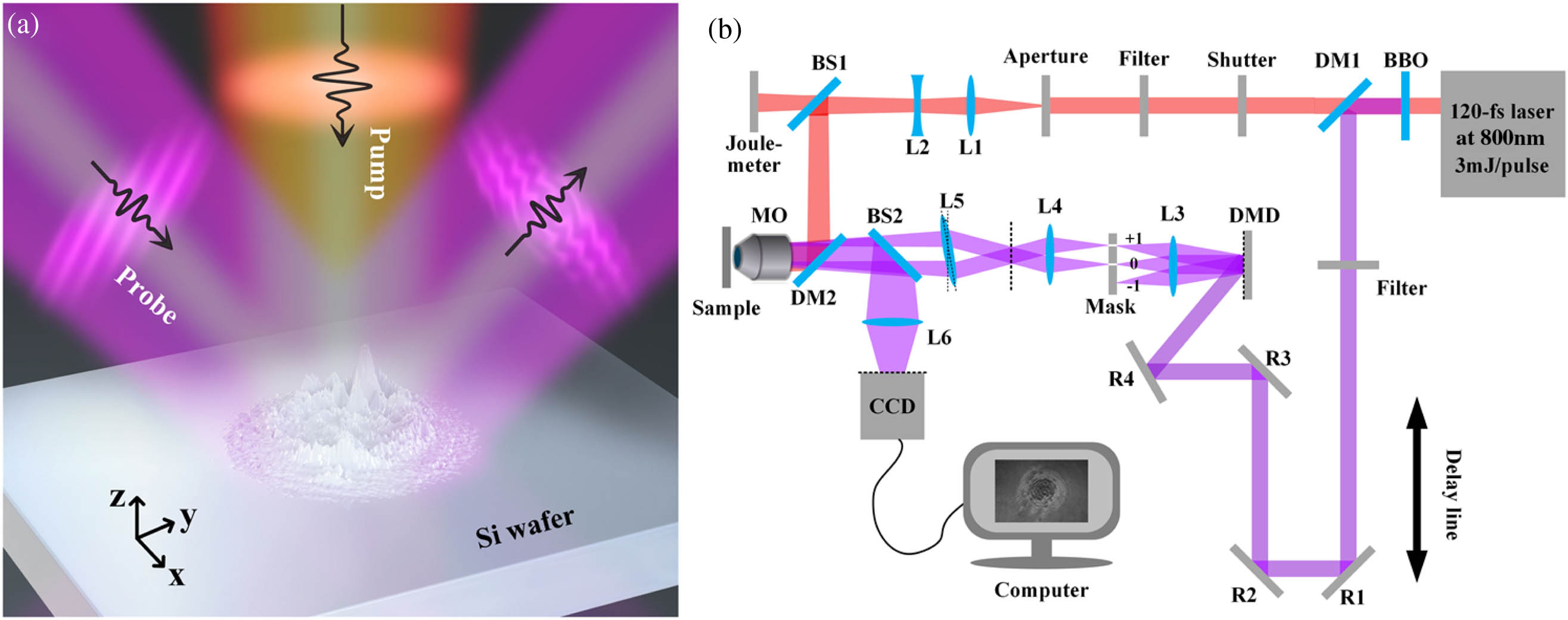
    Fig. 1. Schematic of the SPSLM, where red and violet indicate pump light (at 800 nm) and probe light (at 400 nm), respectively. (a) Diagram of ultrafast pulses on Si wafer. (b) Optical path of SPSLM: BBO, barium boron oxide; DM1, DM2, dichroic mirrors; L1–L6, lenses; R1–R5, reflectors; BS1, BS2, beam splitters; DMD, digital mirror device; CCD, charge-coupled device; MO, microscope objective (100×, apochromatic, NA=0.9).
    Principle and calibration of topography reconstruction. (a) Schematic of illumination light on the field of view formed by interference of the +1st and zeroth orders; (b) fringes in raw image of a polished monocrystalline Si wafer (surface roughness <2 nm) at different planes perpendicular to z axis; (c) grayscale distributions in x direction on CCD, with sample placed at z=0 nm and z=180 nm; (d) phase shift from z=0 to various z positions, as a function of z, indicating the calibration between phase and height.
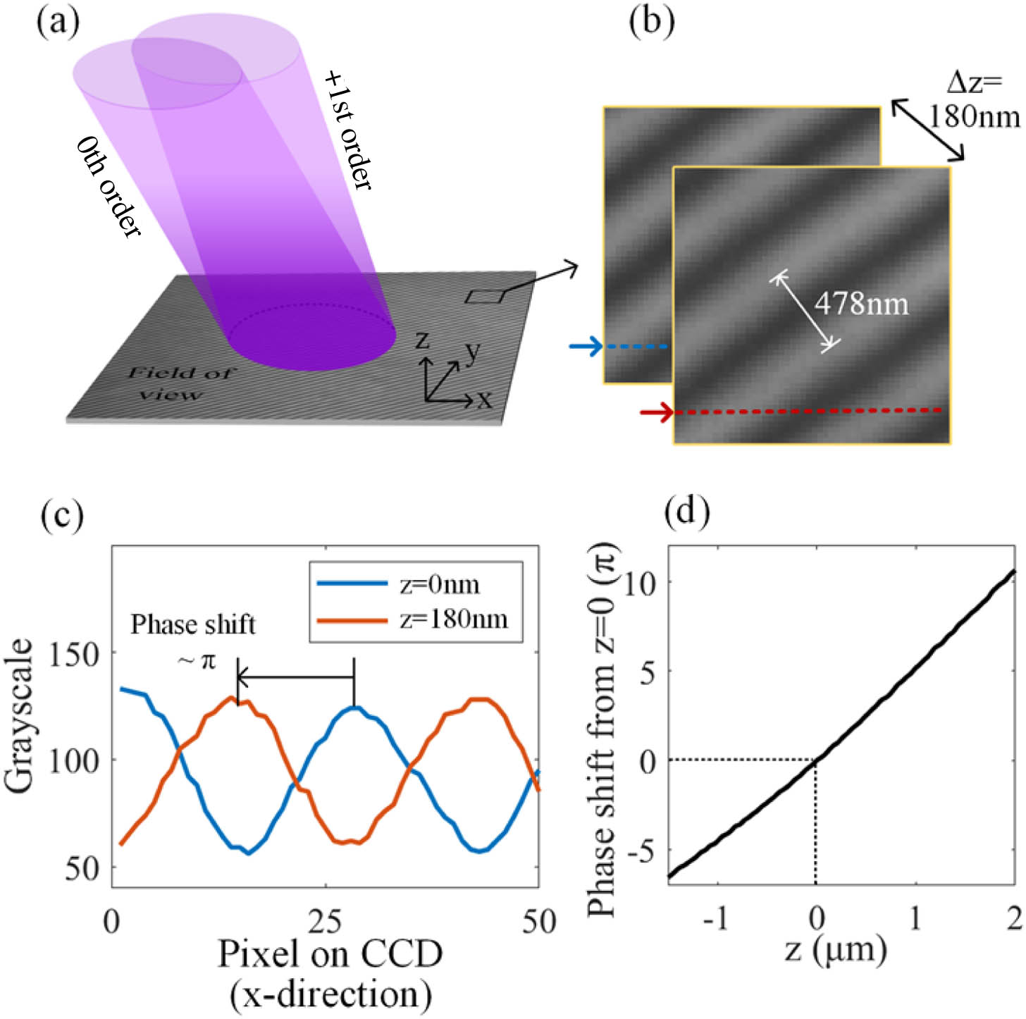
    Fig. 2. Principle and calibration of topography reconstruction. (a) Schematic of illumination light on the field of view formed by interference of the +1st and zeroth orders; (b) fringes in raw image of a polished monocrystalline Si wafer (surface roughness <2  nm) at different planes perpendicular to z axis; (c) grayscale distributions in x direction on CCD, with sample placed at z=0  nm and z=180  nm; (d) phase shift from z=0 to various z positions, as a function of z, indicating the calibration between phase and height.
    Verification of topography reconstruction. (a) Height map of a sample (ablation point on the surface of a polished silicon carbide, containing a pit and LIPSS) obtained via AFM; (b) raw image obtained via SPSLM; (c) reconstructed topography from the raw image; (d) height variations along the dashed lines in (a) and (c) for comparison.
    Fig. 3. Verification of topography reconstruction. (a) Height map of a sample (ablation point on the surface of a polished silicon carbide, containing a pit and LIPSS) obtained via AFM; (b) raw image obtained via SPSLM; (c) reconstructed topography from the raw image; (d) height variations along the dashed lines in (a) and (c) for comparison.
    Raw images (first row) and reconstructed height maps (second row) in time sequence near the zero point with the step of 0.5 ps captured by SPSLM. Pump pulse impacts on Si wafer in the area in orange dashed circle, with average fluence of about 0.29 J/cm2.
    Fig. 4. Raw images (first row) and reconstructed height maps (second row) in time sequence near the zero point with the step of 0.5 ps captured by SPSLM. Pump pulse impacts on Si wafer in the area in orange dashed circle, with average fluence of about 0.29  J/cm2.
    Ultrafast evolution of the topography on Si surface impacted by a single pump pulse with different energies of 266 nJ, 304 nJ, and 382 nJ, corresponding to the average fluences of 0.23 J/cm2, 0.29 J/cm2, and 0.34 J/cm2, respectively (see Visualization 1). The pump light is linearly polarized in the horizontal direction. The final result at a time delay of 100 ms is denoted as “∞.” All other parameters are the same as those in Fig. 4.
    Fig. 5. Ultrafast evolution of the topography on Si surface impacted by a single pump pulse with different energies of 266 nJ, 304 nJ, and 382 nJ, corresponding to the average fluences of 0.23  J/cm2, 0.29  J/cm2, and 0.34  J/cm2, respectively (see Visualization 1). The pump light is linearly polarized in the horizontal direction. The final result at a time delay of 100 ms is denoted as “.” All other parameters are the same as those in Fig. 4.
    Ultrafast topography evolution on the Si surface impacted by second and third pulses (see Visualization 1), and final results compared with AFM. Pulse energy in three groups (separated with black dashed lines) is the same as energies 1–3 in Fig. 5. Pump light is linearly polarized in horizontal direction. Final height maps obtained from SPSLM and from AFM are given for comparison. All other parameters are the same as those in Fig. 5.
    Fig. 6. Ultrafast topography evolution on the Si surface impacted by second and third pulses (see Visualization 1), and final results compared with AFM. Pulse energy in three groups (separated with black dashed lines) is the same as energies 1–3 in Fig. 5. Pump light is linearly polarized in horizontal direction. Final height maps obtained from SPSLM and from AFM are given for comparison. All other parameters are the same as those in Fig. 5.
    Process of FFT to evaluate the quality of LIPSS located in the center region (about 3 μm×3 μm), and the variations of normalized FFT power of point P as a function of time delay after first, second, and third pulses, including the three cases of energies 1–3 (see Visualization 1).
    Fig. 7. Process of FFT to evaluate the quality of LIPSS located in the center region (about 3  μm×3  μm), and the variations of normalized FFT power of point P as a function of time delay after first, second, and third pulses, including the three cases of energies 1–3 (see Visualization 1).
    Jie Xu, Changjun Min, Yuquan Zhang, Jielei Ni, Gengwei Cao, Qianyi Wei, Jianjun Yang, Xiaocong Yuan. Imaging ultrafast evolution of subwavelength-sized topography using single-probe structured light microscopy[J]. Photonics Research, 2022, 10(8): 1900
    Download Citation