• Acta Physica Sinica
  • Vol. 69, Issue 17, 178702-1 (2020)
Chen-Yang Shi1, Guang-Zong Min1, and Xiang-Yang Liu2、*
Author Affiliations
  • 1Research Institute for Biomimetics and Soft Matter,College of Materials, Xiamen University, Xiamen 361005, China
  • 2Faculty of Science, National University of Singapore, Singapore 119077, Singapore
  • show less
    DOI: 10.7498/aps.69.20200617 Cite this Article
    Chen-Yang Shi, Guang-Zong Min, Xiang-Yang Liu. Research progress of protein-based memristor[J]. Acta Physica Sinica, 2020, 69(17): 178702-1 Copy Citation Text show less
    The development of protein material-based memristor.
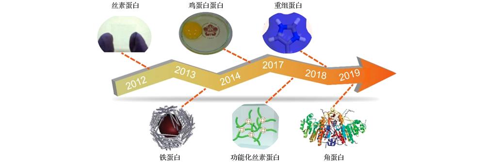
    Fig. 1. The development of protein material-based memristor.
    (a) Schema of sericin memristor; (b) the retention characteristics of the device; (c) typical I-V curves of the device under different compliance currents; (d) the resistance of the device with different compliance currents[33].
    Fig. 2. (a) Schema of sericin memristor; (b) the retention characteristics of the device; (c) typical I-V curves of the device under different compliance currents; (d) the resistance of the device with different compliance currents[33].
    Schema of egg albumen memristor: (a) Proposed fabrication process and schematic of a W/egg albumen/ITO/PET memristor; (b) extracted device HRS and LRS versus bending length; (c) superposition of I-V curves for 3 different memristor cells from the same cross-bar array measured 15 times each; (d) the HRS and LRS resistances of a memristor cell under different temperature with positive bias; general of scheme of peptide bonds (e) and disulfide bonds (f) synthesis between amino acids with different protein chains; (g) schematic drawings of the four switching processes for an albumen-based memristor: (i) Initial state of a memristor with Mg and W as the top and bottom electrode, respectively. The colorful spheres represent different ions; (ii) when a positive voltage is applied to the top electrode, ions move along the electric field, and accumulate locally in strong field regions in the albumen layer; (iii) meanwhile injected electrons from the bottom electrode reduce metallic ions such as Fe3+ and Mg2+ to metal elements. At a specific voltage, the filaments are formed to connect the top and bottom electrodes electrically, and the device is turned on, i.e. the LRS; (iv) when applying a reset voltage, the conductive filaments are broken due to the oxidation of the metal elements by the injected electrons from the top electrode, the filaments are ruptured near the top electrode and the device gradually returns to the HRS[29,32].
    Fig. 3. Schema of egg albumen memristor: (a) Proposed fabrication process and schematic of a W/egg albumen/ITO/PET memristor; (b) extracted device HRS and LRS versus bending length; (c) superposition of I-V curves for 3 different memristor cells from the same cross-bar array measured 15 times each; (d) the HRS and LRS resistances of a memristor cell under different temperature with positive bias; general of scheme of peptide bonds (e) and disulfide bonds (f) synthesis between amino acids with different protein chains; (g) schematic drawings of the four switching processes for an albumen-based memristor: (i) Initial state of a memristor with Mg and W as the top and bottom electrode, respectively. The colorful spheres represent different ions; (ii) when a positive voltage is applied to the top electrode, ions move along the electric field, and accumulate locally in strong field regions in the albumen layer; (iii) meanwhile injected electrons from the bottom electrode reduce metallic ions such as Fe3+ and Mg2+ to metal elements. At a specific voltage, the filaments are formed to connect the top and bottom electrodes electrically, and the device is turned on, i.e. the LRS; (iv) when applying a reset voltage, the conductive filaments are broken due to the oxidation of the metal elements by the injected electrons from the top electrode, the filaments are ruptured near the top electrode and the device gradually returns to the HRS[29,32].
    Ferritin based memristor: (a) Illustration of the fabrication of a single nanorod device with ferritin nanocage spanning OWL-generated about 12 nm gap; (b) ON/OFF ratio of ferritin-based memristive nanodevices with different Fe loading (the color intensity of the protein nanocage core indicates the density of Fe atom); (c) schematic diagram of ferritin, the spherical shell consists of peptide subunits (green) and the mineral core consisting of hydrous iron oxide (orange), lower right panel is the schematic illustration of the Pt/ferritin/Pt memristor on the SiO2/Si substrate; (d) switching voltage distributions of the non-volatile memory; (e) I-V curve and CS-AFM images of (PAH/ferritin)3 multilayers in the ON (Region 3) and OFF state (Region 4) during positive voltage sweep, and the ON (Region 1) and OFF (Region 2) state during negative voltage sweep, respectively. CS-AFM images of multilayer devices were measured from the respective regions in the I-V curve of a (PAH/ferritin)3 multilayer device. The formation of conductive filamentary paths was confirmed by CS-AFM characterizations. In this case, an electrochemically inert Pt tip was used as a top electrode instead of the Ag electrode. The formation and rupture of the randomly distributed paths were observed after “SET” processes (i.e., switching from low-current (OFF) to high-current (ON) state) and “RESET” (i.e., switching from high-current (ON) to low-current (OFF) state)[34,39,40].
    Fig. 4. Ferritin based memristor: (a) Illustration of the fabrication of a single nanorod device with ferritin nanocage spanning OWL-generated about 12 nm gap; (b) ON/OFF ratio of ferritin-based memristive nanodevices with different Fe loading (the color intensity of the protein nanocage core indicates the density of Fe atom); (c) schematic diagram of ferritin, the spherical shell consists of peptide subunits (green) and the mineral core consisting of hydrous iron oxide (orange), lower right panel is the schematic illustration of the Pt/ferritin/Pt memristor on the SiO2/Si substrate; (d) switching voltage distributions of the non-volatile memory; (e) I-V curve and CS-AFM images of (PAH/ferritin)3 multilayers in the ON (Region 3) and OFF state (Region 4) during positive voltage sweep, and the ON (Region 1) and OFF (Region 2) state during negative voltage sweep, respectively. CS-AFM images of multilayer devices were measured from the respective regions in the I-V curve of a (PAH/ferritin)3 multilayer device. The formation of conductive filamentary paths was confirmed by CS-AFM characterizations. In this case, an electrochemically inert Pt tip was used as a top electrode instead of the Ag electrode. The formation and rupture of the randomly distributed paths were observed after “SET” processes (i.e., switching from low-current (OFF) to high-current (ON) state) and “RESET” (i.e., switching from high-current (ON) to low-current (OFF) state)[34,39,40].
    (a) Schema of S-layer protein memristor; (b) endurance characteristics; (c) schematic diagrams of the fabricated rDnaJ device arrays; (d) I-V characteristics of the rDnaJ based memristor; (e) schematic diagram of the CAFM used to observe the conductive filaments. CAFM current mapping image of a conductive filament in the rDnaJ-device after removing the top Cu electrode. The inset shows an enlarged CAFM image of the indicated area; (f) resistance as a function of bending radius for the rDnaJ device fabricated on the flexible PET substrate[35,41].
    Fig. 5. (a) Schema of S-layer protein memristor; (b) endurance characteristics; (c) schematic diagrams of the fabricated rDnaJ device arrays; (d) I-V characteristics of the rDnaJ based memristor; (e) schematic diagram of the CAFM used to observe the conductive filaments. CAFM current mapping image of a conductive filament in the rDnaJ-device after removing the top Cu electrode. The inset shows an enlarged CAFM image of the indicated area; (f) resistance as a function of bending radius for the rDnaJ device fabricated on the flexible PET substrate[35,41].
    (a) Schematic diagrams of keratin from human hair, and the fabrication process of Ag/keratin/FTO memory devices; (b) set and reset voltage distributions collected from eight different devices; (c) the retention characteristics of the device; (d) distribution of the HRS and LRS over 150 consecutive cycles[50,55].
    Fig. 6. (a) Schematic diagrams of keratin from human hair, and the fabrication process of Ag/keratin/FTO memory devices; (b) set and reset voltage distributions collected from eight different devices; (c) the retention characteristics of the device; (d) distribution of the HRS and LRS over 150 consecutive cycles[50,55].
    Silk fibroin-based memristors prepared by Hota’s research group[61]: (a) The I-V characteristics of silk fibroin-based memristors. The corresponding schematic of fabricated memristor device is shown in upper inset. The equivalent circuit model consists of a rectifier in parallel with a memristor is shown in lower inset. (b) Nanoscale conductivity mapping of silk fibroin based memristors under SET and RESET conditions. The STM image shows a higher density of conducting spots or conducting filaments formation during SET condition while those disappear during RESET condition. (c) Proposed physical to explain the switching mechanism of silk fibroin based memristors: (i) Original device conditions, before any bias is applied. (ii) Forming/SET condition is achieved with positive bias. During SET condition local oxidation (SF+) takes place and a soft breakdown event occurs when the density of SF+ reaches a critical value such that a percolation path is formed. (iii) A reset condition is achieved by negative bias. As the conductive SF+ path breaks, the device returns to its fresh-like HRS.
    Fig. 7. Silk fibroin-based memristors prepared by Hota’s research group[61]: (a) The I-V characteristics of silk fibroin-based memristors. The corresponding schematic of fabricated memristor device is shown in upper inset. The equivalent circuit model consists of a rectifier in parallel with a memristor is shown in lower inset. (b) Nanoscale conductivity mapping of silk fibroin based memristors under SET and RESET conditions. The STM image shows a higher density of conducting spots or conducting filaments formation during SET condition while those disappear during RESET condition. (c) Proposed physical to explain the switching mechanism of silk fibroin based memristors: (i) Original device conditions, before any bias is applied. (ii) Forming/SET condition is achieved with positive bias. During SET condition local oxidation (SF+) takes place and a soft breakdown event occurs when the density of SF+ reaches a critical value such that a percolation path is formed. (iii) A reset condition is achieved by negative bias. As the conductive SF+ path breaks, the device returns to its fresh-like HRS.
    The silk fibroin based memristor: (a) Model of silk fibroin based memristor; (b) I-V characteristic curve of the silk fibroin based memristor; (c) the corresponding retention characteristics of the device; (d) the photograph display of a 2 cm × 2 cm memristor that can be sustained by a human hair; (e) I-V characteristic curve of the light silk fibroin-based memristor; (f) the corresponding retention characteristics of the device; (g) schematic of the transient resistive switching memory device, Mg has good biocompatibility and is soluble in water and physiological environment; (h), (i)time sequence of dissolution of the memory devices in DI water at room temperature; (j) scanning electron microscope image of a single silk fibroin-based memory cell in a 12 × 12 array cell, a single silk fibroin pattern is sandwiched between the bottom and top electrodes; (k) the fabricated memristor array is scrolled on a cylinder with a radius of curvature of 1.3 mm; (l) I-V characteristics of silk fibroin arrays[63-66].
    Fig. 8. The silk fibroin based memristor: (a) Model of silk fibroin based memristor; (b) I-V characteristic curve of the silk fibroin based memristor; (c) the corresponding retention characteristics of the device; (d) the photograph display of a 2 cm × 2 cm memristor that can be sustained by a human hair; (e) I-V characteristic curve of the light silk fibroin-based memristor; (f) the corresponding retention characteristics of the device; (g) schematic of the transient resistive switching memory device, Mg has good biocompatibility and is soluble in water and physiological environment; (h), (i)time sequence of dissolution of the memory devices in DI water at room temperature; (j) scanning electron microscope image of a single silk fibroin-based memory cell in a 12 × 12 array cell, a single silk fibroin pattern is sandwiched between the bottom and top electrodes; (k) the fabricated memristor array is scrolled on a cylinder with a radius of curvature of 1.3 mm; (l) I-V characteristics of silk fibroin arrays[63-66].
    Scheme of electron transport in mesoscopic materials: (a) TEM image of AgNCs@BSA showing a core size of 3−4 nm. AFM topographic image (b) and KPFM image (c) of a AgNC (white circles)-functionalized SF film, the electronic wells (b) are 200 nm in size and (c) have a much lower electric potential due to the accumulation of electrons at the surface, the nano seeds (AgNCs) is 30% (the applied voltage is 500 mV, and the gap between the tip and the sample is 100 nm); (d) the corresponding electric potential; (e) the simulation of Poisson-Nernest-Planck; steady state Ag ion and electron density distributions without (f) and with (g) AgNC; (h) scheme of new mesoscopic functionalized SF materials (left side) and the barrier of metal ion migration (right side); (i) scheme of ion transport under an electric field in new mesoscopic functionalized SF materials (left side) and the corresponding schema of different ion transport paths (right side). Two paths to overcome a high potential barrier of metal ion migration (∆G*) (path 1, blue curve) and a lower potential barrier (∆G'*) (path 2, green curve)[24].
    Fig. 9. Scheme of electron transport in mesoscopic materials: (a) TEM image of AgNCs@BSA showing a core size of 3−4 nm. AFM topographic image (b) and KPFM image (c) of a AgNC (white circles)-functionalized SF film, the electronic wells (b) are 200 nm in size and (c) have a much lower electric potential due to the accumulation of electrons at the surface, the nano seeds (AgNCs) is 30% (the applied voltage is 500 mV, and the gap between the tip and the sample is 100 nm); (d) the corresponding electric potential; (e) the simulation of Poisson-Nernest-Planck; steady state Ag ion and electron density distributions without (f) and with (g) AgNC; (h) scheme of new mesoscopic functionalized SF materials (left side) and the barrier of metal ion migration (right side); (i) scheme of ion transport under an electric field in new mesoscopic functionalized SF materials (left side) and the corresponding schema of different ion transport paths (right side). Two paths to overcome a high potential barrier of metal ion migration (∆G*) (path 1, blue curve) and a lower potential barrier (∆G'*) (path 2, green curve)[24].
    Mesoscopic functionalization strategies were used to construct Au-doped silk fibroin-based memristors by Liu's group[68]: (a) Schema of meso-functionalized silk memristor; (b) the 100 times I-V curve of Ag/WK@AuNCs-silk fibroin/ITO, measured by applying voltage to the top Ag electrode while keeping the ITO bottom electrode grounded; (c) the I-V curve of the Ag/neat-silk fibroin/ITO device; (d), (e) the electric potential images of a silk fibroin film functionalized by WK@AuNCs (dot line circles), a much lower electric potential due to the accumulation of electrons at the surfaces (the applied voltage: 500 mV, and the gap between the tip and the sample: 100 nm); (f) the WK@AuNCs-silk fibroin memristor was dissolved completed by the papain solution while the one in water was stable; (g) schema of the conduction mechanism of the Ag/WK@AuNCs-silk fibroin/ITO device. Ag ions move from the Ag electrode through the silk fibroin film toward the ITO electrode with the assistance of the AuNCs. Ag ions bridged by the AuNCs are reduced in the ITO electrode.
    Fig. 10. Mesoscopic functionalization strategies were used to construct Au-doped silk fibroin-based memristors by Liu's group[68]: (a) Schema of meso-functionalized silk memristor; (b) the 100 times I-V curve of Ag/WK@AuNCs-silk fibroin/ITO, measured by applying voltage to the top Ag electrode while keeping the ITO bottom electrode grounded; (c) the I-V curve of the Ag/neat-silk fibroin/ITO device; (d), (e) the electric potential images of a silk fibroin film functionalized by WK@AuNCs (dot line circles), a much lower electric potential due to the accumulation of electrons at the surfaces (the applied voltage: 500 mV, and the gap between the tip and the sample: 100 nm); (f) the WK@AuNCs-silk fibroin memristor was dissolved completed by the papain solution while the one in water was stable; (g) schema of the conduction mechanism of the Ag/WK@AuNCs-silk fibroin/ITO device. Ag ions move from the Ag electrode through the silk fibroin film toward the ITO electrode with the assistance of the AuNCs. Ag ions bridged by the AuNCs are reduced in the ITO electrode.
    Electronic characteristics of meso-devices: (a) Typical current-voltage (I-V) characteristics of silk fibroin-based memory devices, the resistance switches from the HRS to LRS through a “set” process, and the state can be reversed via a “reset” step; I-V curves of (b) Ag0 and (c) Ag30; (d) distribution of the resistance of neat silk fibroin (blue) and functionalized silk fibroin (yellow) devices at the HRS and LRS; (e) distribution of the set and reset voltages in neat silk fibroin (blue) and functionalized silk fibroin (yellow) devices; (f) the distributions of Vset, Vreset, and OFF/ON ratio as a function of the amount of Ag used to functionalize the switching layer; switching speed of the functionalized silk fibroin memristor, the write/erase speeds are (g) 15 ns and (h) 10 ns, respectively; (i) comparison of operating voltages for different organic storage media. The set/reset voltage of the meso-functionalized silk fibroin memristor is reduced about 40 times (from 12 to 0.3 V) compared with the neat silk fibroin memristor; (j) comparison of write/erase speeds for different categories of storage media. The write/erase speed of the meso-functionalized silk fibroin memristor is improved about 10 times (from 100 to 10 ns) compared with other reported protein memristors[24].
    Fig. 11. Electronic characteristics of meso-devices: (a) Typical current-voltage (I-V) characteristics of silk fibroin-based memory devices, the resistance switches from the HRS to LRS through a “set” process, and the state can be reversed via a “reset” step; I-V curves of (b) Ag0 and (c) Ag30; (d) distribution of the resistance of neat silk fibroin (blue) and functionalized silk fibroin (yellow) devices at the HRS and LRS; (e) distribution of the set and reset voltages in neat silk fibroin (blue) and functionalized silk fibroin (yellow) devices; (f) the distributions of Vset, Vreset, and OFF/ON ratio as a function of the amount of Ag used to functionalize the switching layer; switching speed of the functionalized silk fibroin memristor, the write/erase speeds are (g) 15 ns and (h) 10 ns, respectively; (i) comparison of operating voltages for different organic storage media. The set/reset voltage of the meso-functionalized silk fibroin memristor is reduced about 40 times (from 12 to 0.3 V) compared with the neat silk fibroin memristor; (j) comparison of write/erase speeds for different categories of storage media. The write/erase speed of the meso-functionalized silk fibroin memristor is improved about 10 times (from 100 to 10 ns) compared with other reported protein memristors[24].
    Schematic structure diagrams illustrating resistances switching mechanism in the pure SF memristor: (a) Initial state; (b) HRS state during corresponding positive sweeps; (c) LRS state, conductive filaments are formed in LRS state during corresponding set sweeps; (d) the device switches to HRS when applied reset voltage corresponds to rupture of the conductive filaments; (e) HRS state during corresponding negative sweeps; (f) the random conductive filaments formed in subsequent repeated sweeps under an electric field; (g) endurance cycles of neat SF memristor[24].
    Fig. 12. Schematic structure diagrams illustrating resistances switching mechanism in the pure SF memristor: (a) Initial state; (b) HRS state during corresponding positive sweeps; (c) LRS state, conductive filaments are formed in LRS state during corresponding set sweeps; (d) the device switches to HRS when applied reset voltage corresponds to rupture of the conductive filaments; (e) HRS state during corresponding negative sweeps; (f) the random conductive filaments formed in subsequent repeated sweeps under an electric field; (g) endurance cycles of neat SF memristor[24].
    Schematic structure diagrams illustrating the resistance switching mechanism in AgNC meso-functionalized devices. (a) Current-voltage diagrams representing the resistance state during step-by-step changes in the electric field. (b) Schematic of filament growth dynamics corresponding to the resistance state. The red Ag clusters in the schematic represent mesoscopic functionali-zation in the memristive material; these clusters can act as a positive charge trap when polarized by an external electric field. The arrows indicate the switching direction: (i) Initial state; (ii) HRS state during corresponding positive sweeps; (iii) LRS state, conductive filaments are formed in the LRS state during corresponding set sweeps; (iv) the device remains in the LRS when the applied reverse voltage corresponds to the dissolution of the conductive filaments; (v) the device switches to the HRS when the applied reverse voltage reaches the reset voltage, which corresponds to the rupture of the conductive filaments; (vi) HRS state during corresponding negative sweeps. Well-organized conductive filaments are formed in subsequent repeated sweeps under an electric field. (c) Endurance cycles of Meso-functionalized silk fibroin memristor[24].
    Fig. 13. Schematic structure diagrams illustrating the resistance switching mechanism in AgNC meso-functionalized devices. (a) Current-voltage diagrams representing the resistance state during step-by-step changes in the electric field. (b) Schematic of filament growth dynamics corresponding to the resistance state. The red Ag clusters in the schematic represent mesoscopic functionali-zation in the memristive material; these clusters can act as a positive charge trap when polarized by an external electric field. The arrows indicate the switching direction: (i) Initial state; (ii) HRS state during corresponding positive sweeps; (iii) LRS state, conductive filaments are formed in the LRS state during corresponding set sweeps; (iv) the device remains in the LRS when the applied reverse voltage corresponds to the dissolution of the conductive filaments; (v) the device switches to the HRS when the applied reverse voltage reaches the reset voltage, which corresponds to the rupture of the conductive filaments; (vi) HRS state during corresponding negative sweeps. Well-organized conductive filaments are formed in subsequent repeated sweeps under an electric field. (c) Endurance cycles of Meso-functionalized silk fibroin memristor[24].
    Carbon dots(CDs)-doped silk fibroin-based memristors: (a) Cross-sectional SEM image of the device structure; (b) TEM images of pristine CDs; (c) AFM topographic images of CDs-silk composite film on a mica substrate, scale bar is 300 nm; (d) Ag top electrode, exposed to UV light (λ = 365 nm) with intensity from 0 to 0.15 Mw/cm2 (sweeping rate is 50 mV); (e) distribution of SET voltages without (left) and with (right) UV light treatment; (f) an enlarged SEM image of the conductive filament and EDS spectra in different regions; (g) cross-sectional SEM image of the Au/pentacene/CDs/silk/SiO2/Si device; (h) AFM topographic images of the CDs/silk bicomponent blend film; (i) output characteristics of the memory under dark conditions (left panel) and light illumination (right panel, λ = 365 nm, light intensity: 0.15 Mw/cm2); (j) KPFM image of CDs/silk film after electrons injection through incrementally increasing voltage applied to the tip under dark (left panel) and under UV illumination (right panel); (k) the CPD value of the selected cross sections in (j)[70,71].
    Fig. 14. Carbon dots(CDs)-doped silk fibroin-based memristors: (a) Cross-sectional SEM image of the device structure; (b) TEM images of pristine CDs; (c) AFM topographic images of CDs-silk composite film on a mica substrate, scale bar is 300 nm; (d) Ag top electrode, exposed to UV light (λ = 365 nm) with intensity from 0 to 0.15 Mw/cm2 (sweeping rate is 50 mV); (e) distribution of SET voltages without (left) and with (right) UV light treatment; (f) an enlarged SEM image of the conductive filament and EDS spectra in different regions; (g) cross-sectional SEM image of the Au/pentacene/CDs/silk/SiO2/Si device; (h) AFM topographic images of the CDs/silk bicomponent blend film; (i) output characteristics of the memory under dark conditions (left panel) and light illumination (right panel, λ = 365 nm, light intensity: 0.15 Mw/cm2); (j) KPFM image of CDs/silk film after electrons injection through incrementally increasing voltage applied to the tip under dark (left panel) and under UV illumination (right panel); (k) the CPD value of the selected cross sections in (j)[70,71].
    Other functionalized silk fibroin based memristors: (a) Schema of Au nanoparticles functionalized silk memristor; (b) I-V switching characteristics of the ITO/silk fibroin-Au/Al device and the pure silk device (in the inset); (c) schema of CdSe-silk memristor; (d) multilevel memory switching of CdSe-silk memristor[72,73].
    Fig. 15. Other functionalized silk fibroin based memristors: (a) Schema of Au nanoparticles functionalized silk memristor; (b) I-V switching characteristics of the ITO/silk fibroin-Au/Al device and the pure silk device (in the inset); (c) schema of CdSe-silk memristor; (d) multilevel memory switching of CdSe-silk memristor[72,73].
    器件结构开关比开关电压/V保持时长/s擦写速度/ns循环次数
    Al/蚕丝蛋白/ITO[61]1010.4/–11.5
    Ag/蚕丝蛋白/Au[63]1071.3—3.4/–1.34.5 × 103
    Ag/蚕丝蛋白/Au[64]1050.7—1.7/–1.210430
    Mg/蚕丝蛋白/Mg[65]1040.7—1.7/–110450
    Au/蚕丝蛋白/Pt[74]1043/–1.75.7 × 10330
    Al/CdSe-蚕丝蛋白/ITO[73]104
    Ag/Au-蚕丝蛋白/ITO[68]1020.4/–0.21.4 × 104100
    Ag/Ag-蚕丝蛋白/ITO[24]1030.3/–0.1810410100
    Al/CDs-蚕丝蛋白/ITO[70]3/–1106100
    W/鸡蛋白蛋白/ITO[32]1022/7100
    Ag/鸡蛋白蛋白/Al[75]1020.6/–0.71047550
    Pt/铁蛋白/Pt[34]1052.2/–1.16 × 10370
    Ag/丝胶蛋白/Au[33]1062.5/–0.810321
    Al/S-layer/ITO[35]6.28/–84 × 103500
    Cu/rDnaj/Pt[41]1060.12/–0.08106100
    Ag/角蛋白/FTO[50]1031.5/–1.5104100
    Ag/溶菌酶/Pt[47]1061/–1.3104100200
    Table 1. The comparison of protein-based memristors.
    Chen-Yang Shi, Guang-Zong Min, Xiang-Yang Liu. Research progress of protein-based memristor[J]. Acta Physica Sinica, 2020, 69(17): 178702-1
    Download Citation