• Chinese Optics Letters
  • Vol. 18, Issue 6, 061301 (2020)
Yaru Han1, Bing Xiong1、2、*, Changzheng Sun1、2, Zhibiao Hao1、2, Jian Wang1、2, Yanjun Han1、2、3, Lai Wang1、2, Hongtao Li1、2, Jiadong Yu1、2、3, and Yi Luo1、2、3
Author Affiliations
  • 1Beijing National Research Center for Information Science and Technology (BNRist), Department of Electronic Engineering, Tsinghua University, Beijing 100084, China
  • 2Center for Flexible Electronics Technology, Tsinghua University, Beijing 100084, China
  • 3Flexible Intelligent Optoelectronic Device and Technology Center, Institute of Flexible Electronics Technology of THU, Jiaxing 314006, China
  • show less
    DOI: 10.3788/COL202018.061301 Cite this Article Set citation alerts
    Yaru Han, Bing Xiong, Changzheng Sun, Zhibiao Hao, Jian Wang, Yanjun Han, Lai Wang, Hongtao Li, Jiadong Yu, Yi Luo. Distributed parameter circuit model for wideband photodiodes with inductive coplanar waveguide electrodes[J]. Chinese Optics Letters, 2020, 18(6): 061301 Copy Citation Text show less
    (a) Schematic diagram and (b) equivalent circuit model of the CPW. (c) The equivalent circuit model of the PD. Region 1 represents the transit time parameters, Region 2 represents the bulk and parasitic parameters of the PD, and Region 3 represents the n-section distributed parameter model of the CPW. The box on the left represents the intrinsic bandwidth parameters.
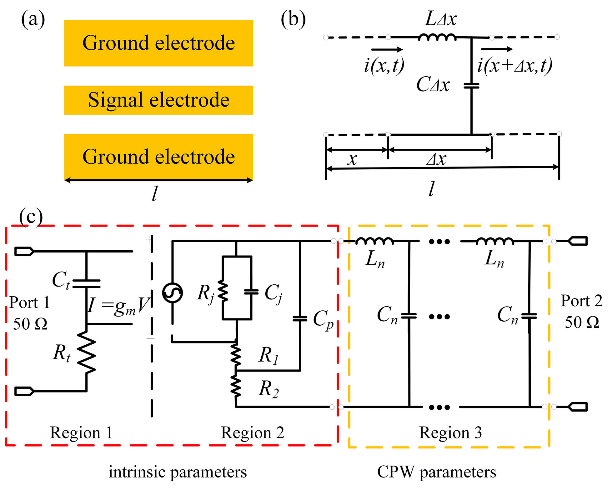
    Fig. 1. (a) Schematic diagram and (b) equivalent circuit model of the CPW. (c) The equivalent circuit model of the PD. Region 1 represents the transit time parameters, Region 2 represents the bulk and parasitic parameters of the PD, and Region 3 represents the n-section distributed parameter model of the CPW. The box on the left represents the intrinsic bandwidth parameters.
    Two different CPW structures: (a) CPW-1 with 50 Ω impedance; (b) CPW-2 containing an inductive high-impedance part. The FEM simulated S11 and S21 parameters of (c) CPW-1 and (d) CPW-2 up to 40 GHz. The extracted distributed parameters (e) L and (f) C of the designed CPW-1 and CPW-2.
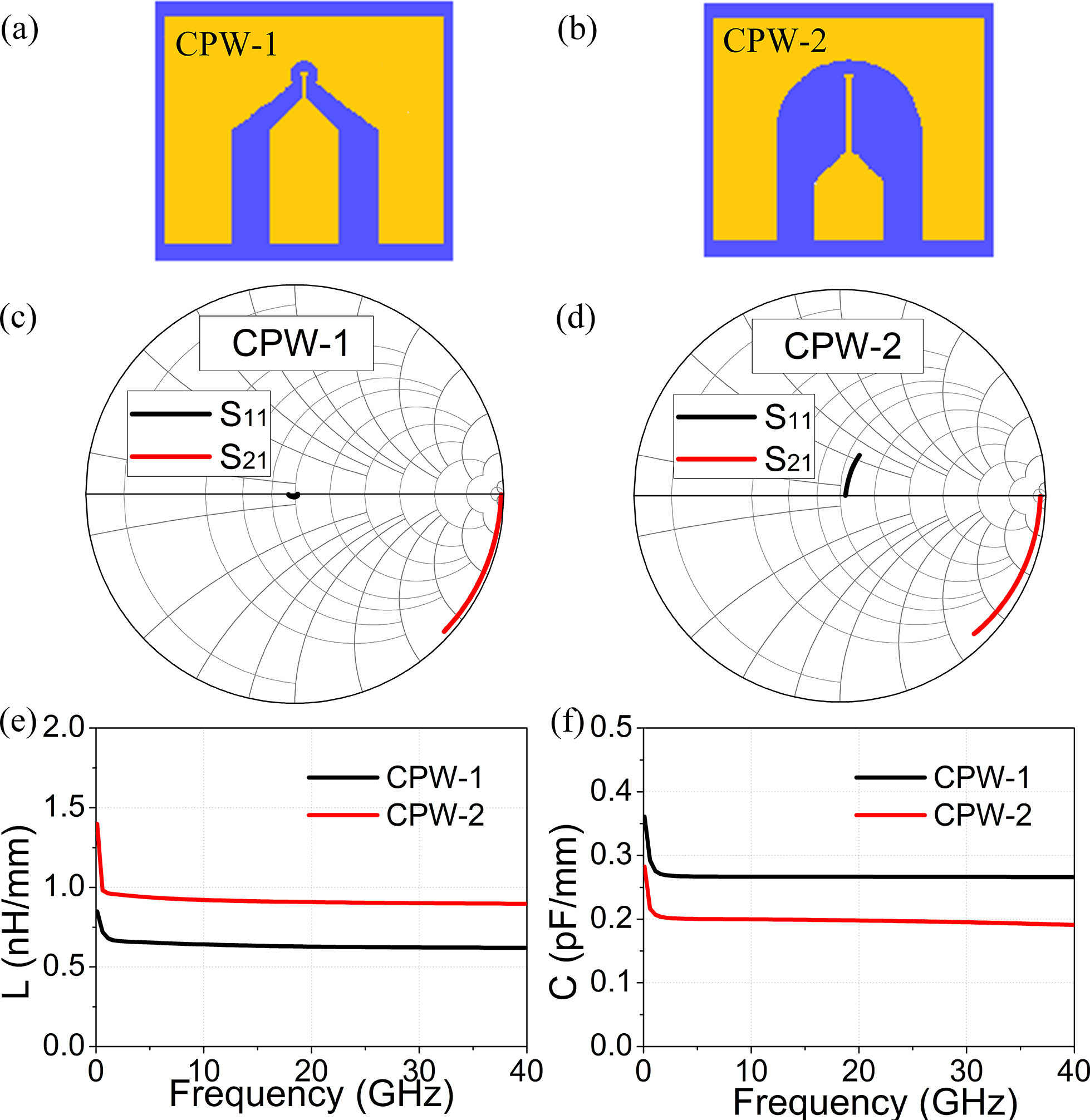
    Fig. 2. Two different CPW structures: (a) CPW-1 with 50Ω impedance; (b) CPW-2 containing an inductive high-impedance part. The FEM simulated S11 and S21 parameters of (c) CPW-1 and (d) CPW-2 up to 40 GHz. The extracted distributed parameters (e) L and (f) C of the designed CPW-1 and CPW-2.
    Fitted S11 and S21 parameters of the 3-section circuit model of (a) CPW-1 and (b) CPW-2.
    Fig. 3. Fitted S11 and S21 parameters of the 3-section circuit model of (a) CPW-1 and (b) CPW-2.
    Top view of the PDs with the (a) CPW-1 and (b) CPW-2 structures, (c) the schematic device structure[16], and (d) the epitaxial layers of the MUTC-PD.
    Fig. 4. Top view of the PDs with the (a) CPW-1 and (b) CPW-2 structures, (c) the schematic device structure[16], and (d) the epitaxial layers of the MUTC-PD.
    (a) Measured and fitted frequency response at a reverse bias of 5 V and a photocurrent of 35 mA. (b) The output RF power versus the DC photocurrent at 40 GHz under a reverse bias of 5 V. (c) The 3 dB bandwidth under different biases and a fixed photocurrent of 35 mA. (d) The bandwidth improvement of PD-2 over that of PD-1.
    Fig. 5. (a) Measured and fitted frequency response at a reverse bias of 5 V and a photocurrent of 35 mA. (b) The output RF power versus the DC photocurrent at 40 GHz under a reverse bias of 5 V. (c) The 3 dB bandwidth under different biases and a fixed photocurrent of 35 mA. (d) The bandwidth improvement of PD-2 over that of PD-1.
    Measured and fitted S22 parameters (0–40 GHz) of (a) PD-1 and (b) PD-2 with different CPWs at a reverse bias of 5 V and a photocurrent of 35 mA. Also, the measured S22 parameters of (c) PD-1 and (d) PD-2 under different biases.
    Fig. 6. Measured and fitted S22 parameters (0–40 GHz) of (a) PD-1 and (b) PD-2 with different CPWs at a reverse bias of 5 V and a photocurrent of 35 mA. Also, the measured S22 parameters of (c) PD-1 and (d) PD-2 under different biases.
    3 dB bandwidth limited by the transit time and RC constant of PD-1 and PD-2 under different bias voltages.
    Fig. 7. 3 dB bandwidth limited by the transit time and RC constant of PD-1 and PD-2 under different bias voltages.
    (a) Frequency responses of the PDs under a bias voltage of 5 V. (b) Frequency responses of the PDs with and without the CPW electrodes.
    Fig. 8. (a) Frequency responses of the PDs under a bias voltage of 5 V. (b) Frequency responses of the PDs with and without the CPW electrodes.
    StructureSections (n)Ln (pH)Cn (pF)
    CPW-13450.020
    CPW-23700.015
    Table 1. Parameters of 3-Section Model (Region 3)
    PD-1PD-2Rt(Ω)Ct(pF)Rj(Ω)Cj(fF)R1(Ω)R2(Ω)Cp(fF)
    2 V70351800635105.5
    3 V60355500525105.5
    4 V5635104485105.5
    5 V5635105445105.5
    6 V5635105445105.5
    Table 2. Intrinsic Parameters of PDs in Region 1 and Region 2
    Yaru Han, Bing Xiong, Changzheng Sun, Zhibiao Hao, Jian Wang, Yanjun Han, Lai Wang, Hongtao Li, Jiadong Yu, Yi Luo. Distributed parameter circuit model for wideband photodiodes with inductive coplanar waveguide electrodes[J]. Chinese Optics Letters, 2020, 18(6): 061301
    Download Citation