1Beijing National Research Center for Information Science and Technology (BNRist), Department of Electronic Engineering, Tsinghua University, Beijing 100084, China
2Center for Flexible Electronics Technology, Tsinghua University, Beijing 100084, China
3Flexible Intelligent Optoelectronic Device and Technology Center, Institute of Flexible Electronics Technology of THU, Jiaxing 314006, China
An equivalent circuit model including multi-section distributed parameters is proposed to analyze wideband photodiodes (PDs) with coplanar waveguide (CPW) electrodes. The model helps extract CPW parameters as well as intrinsic bandwidth parameters so that the influence of the CPW structure can be investigated, making it valuable for the design of high-performance PDs. PDs with an inductive 115 Ω impedance CPW are fabricated, and the 3 dB bandwidth is improved from 28 GHz to 37.5 GHz compared with PDs with a conventional 50 Ω impedance CPW.
High-power and wideband photodiodes (PDs) are key components for microwave photonic applications such as optically controlled phased array antennas, wireless over-fiber systems, and optical/mm-wave access networks[1–3]. PDs with a wideband and high-power handling capacity help improve analog optical link performance such as link gain, noise figure, and spurious-free dynamic range (SFDR). A thin absorption layer is needed for high-speed performance, but it will cause a low responsivity[4]. Reducing the active area (i.e., RC constant) of the PD is one effective way to improve the bandwidth performance, but it will lead to a reduction in the output saturation power. Various device structures have been proposed to overcome the trade-off between bandwidth and saturation characteristics such as the charge compensation modified uni-traveling-carrier (CC-MUTC) structure[5,6], double depletion layer (DDL) structure[7], and near-ballistic UTC structure[8,9]. Resonant circuits have been adopted to improve the output RF power, but the frequency range is narrow[10,11]. PDs with high-impedance coplanar waveguide (CPW) electrodes show improved frequency response and output power performance simultaneously over PDs with a conventional CPW[12–14]. Such devices take advantage of the inductance of the high-impedance CPW to compensate the junction capacitance of the PD. Device parameters such as the transit time, junction capacitance, and parasitic parameters of the PD are important for the design of the high-impedance CPW. Both the impedance and the length of the CPW will affect the frequency response of the device. For high-power PDs with a CPW, an equivalent circuit model with photocurrent-dependent RC parameters has been established to analyze the device performance under different working conditions[15]. However, the model needs to be extended to take the CPW parameters into account to make it suitable for high-impedance CPW-based high-power PDs.
In this Letter, an equivalent circuit model is proposed to analyze the influence of the CPW structure on the frequency response of PDs in which multi-section distributed parameters are included to model the CPW structure. An -section distributed parameter circuit model is tuned to fit the simulated S-parameters of the CWP structure obtained with the finite element method (FEM), and the appropriate number of sections is determined accordingly. Intrinsic PD parameters, such as the transit time and parasitic parameter, can then be obtained by fitting the measured and parameters of the PD based on our previous analysis model[15]. The proposed model helps to distinguish the influence of CPW parameters from those of the transit time and RC constant on the bandwidth performance of the PD.
As an example, two PDs with the same size but different CPW structures are frabricated and analyzed. PD-1, with a conventional impedance CPW structure, shows a 3 dB bandwidth of 28 GHz while PD-2, with an inductive high-impedance CPW structure, exhibits an improved 3 dB bandwidth of 37.5 GHz. The saturation output RF powers at 40 GHz are 15 and 17 dBm, respectively. The fitted results obtained with the proposed model are in good agreement with the experimental data, and the influence of the CPW on the bandwidth performance of the PD can be analyzed in detail.
Sign up for Chinese Optics Letters TOC. Get the latest issue of Chinese Optics Letters delivered right to you!Sign up now
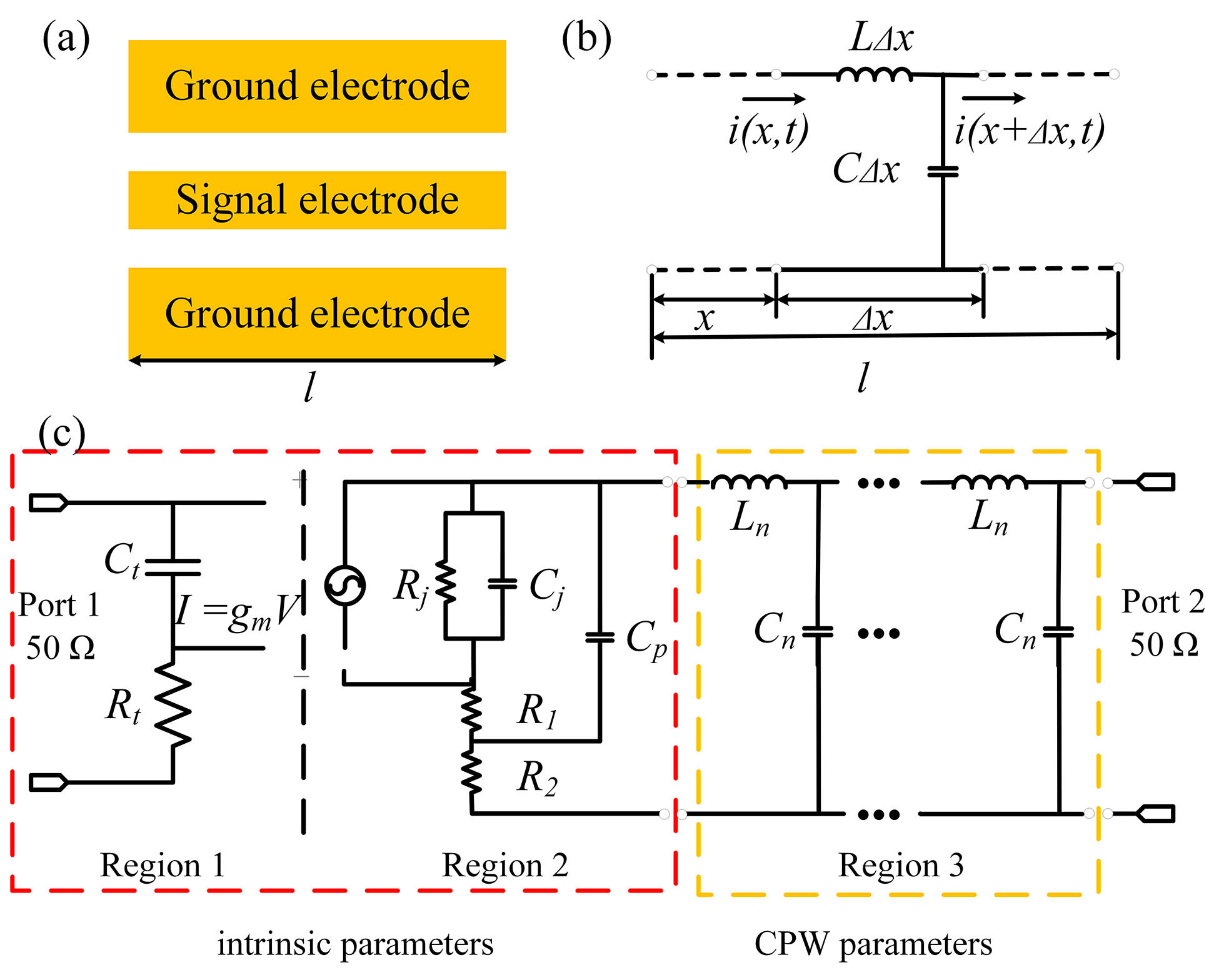
The schematic diagram and the multi-section equivalent circuit model of the CPW are shown in Figs. 1(a) and 1(b), respectively. Here, is the series inductance per unit length, while is the shunt capacitance per unit length.
Figure 1.(a) Schematic diagram and (b) equivalent circuit model of the CPW. (c) The equivalent circuit model of the PD. Region 1 represents the transit time parameters, Region 2 represents the bulk and parasitic parameters of the PD, and Region 3 represents the -section distributed parameter model of the CPW. The box on the left represents the intrinsic bandwidth parameters.
The circuit model for the entire PD is given in Fig. 1(c), where the CPW is modeled by an -section equivalent circuit with parameters and to ensure a sufficient accuracy. and are used to describe the effect of the transit time. and are the junction resistance and junction capacitance, respectively, which can vary under different working conditions[15]. is the bulk resistance and is the ohmic contact resistance. is the parasitic capacitance.
The distributed parameters ( and ), as well as the number of sections () of the CPW, can be determined as follows. According to the telegraph equation, the characteristic impedance and propagation constant can be expressed in terms of the S-parameters of a single section as where is the propagation constant of the microwave signal, is the load, and is total length of the CPW. The propagation constant and the characteristic impedance are related to the distributed parameters as
As a result, and can be extracted as
Once the distributed and parameters are obtained, the -section model is tuned to fit the S-parameters and the appropriate number of sections () is adopted to make the model accurate yet simple. Compared with the single-section equivalent circuit model, the multi-section model is only a series of cascaded single sections and tends to provide a better fitting to the S-parameters of the CPW. The parameters and for the -section circuit model are related to the single-section circuit model parameters and as
To better understand the model, two CPW structures are designed, as shown in Fig. 2. CPW-1 is designed to match with the load, with a signal electrode width of 97 μm and a gap of 50 μm. CPW-2 includes an inductive high-impedance part to match with the junction capacitance of the PD. The 100-μm-long high-impedance part is designed with a signal width of 6 μm and a gap of 97 μm to obtain a characteristic impedance. Both structures contain a 50-μm-long impedance gradient change part. The total length of both CPWs is 230 μm. In the following part, the effect of the high-impedance CPW on the PD’s frequency response will be analyzed in detail.
Figure 2.Two different CPW structures: (a) CPW-1 with impedance; (b) CPW-2 containing an inductive high-impedance part. The FEM simulated and parameters of (c) CPW-1 and (d) CPW-2 up to 40 GHz. The extracted distributed parameters (e) and (f) of the designed CPW-1 and CPW-2.
First, the and parameters of CPW-1 and CPW-2 are obtained with the FEM simulation. In our simulation, the size of the device is , while the size of the air box is . The ports are excited with a load, the maximum simulation frequency is 40 GHz, and the solution frequency is 40 GHz. As shown in Fig. 2(c), CPW-1 is well matched with the ports, and the transmission loss can almost be ignored. CPW-2 contains a high-impedance part and exhibits a higher transmission loss due to the impedance mismatch. Based on the CPW’s S-parameters, the distributed parameters of the CPWs can be extracted, as shown in Figs. 2(e) and 2(f). In the extraction process, the impedance is kept as a constant. The extracted and of CPW-1 are 0.62 nH/mm and 0.27 pF/mm, respectively, whereas the extracted and of CPW-2 are 0.9 nH/mm and 0.19 pF/mm, respectively. The high-impedance CPW shows more inductive characteristics than the conventional CPW-1.
From the distributed parameters, the -section distributed parameters ( and ) of the CPW in the circuit can be obtained, as shown in Table 1. The simulated S-parameters of the -section model (Region 3) are shown in Fig. 3. The S-parameters calculated with the 3-section model fit well with those obtained by FEM simulation. Thus, the distributed parameters of CPW-1 and CPW-2 are extracted based on the above analysis. The equivalent length of each section is 76.7 μm, which is much shorter than the wavelength of the 40 GHz signal (2.1 mm on InP substrate), resulting in a relatively accurate result.
Once the 3-section circuit parameters of the CPW are determined, as shown in Table 1, the influence of the CPW on the frequency response of the PDs can be clearly analyzed.
As an example, backside-illuminated PDs with the two different CPWs are fabricated on the same wafer, as shown in Figs. 4(a)–4(c). The epitaxial layers of the MUTC-PD are shown in Fig. 4(d). The absorption region includes a 650-nm-thick graded p-doped InGaAs layer and a 200-nm-thick n-doped InGaAs layer. The total 850-nm-thick InGaAs absorption region will result in a high responsivity. The depletion region includes a 200-nm-thick InGaAs layer and a 620-nm-thick InP layer. Two 20-nm-thick n-cliff InP layers are inserted into the InP depletion region to shield the space charge effect, to improve the saturation characteristics[6,16].
Figure 4.Top view of the PDs with the (a) CPW-1 and (b) CPW-2 structures, (c) the schematic device structure[16], and (d) the epitaxial layers of the MUTC-PD.
P- and n-mesas are patterned by combined inductively coupled plasma (ICP) dry-etching and wet-etching processes. Ti/Pt/Au and Ni/Au are sputtered as p- and n-electrodes, respectively. An 800-nm-thick is deposited to reduce the surface leakage current and parasitic capacitance. A 1.5-μm-thick CPW electrode is formed on top of the layer by electroplating. Finally, the device is thinned and back polished, and a 215 nm is deposited to reduce the reflection of the incident light.
The frequency response and the saturation characteristics of the PDs are measured with 100% modulated light generated through the two-laser heterodyne method[17]. A distributed feedback laser (Avanex A1905LMI) and a tunable laser (Santec TSL-210 V) are heterodyned to get the 100% modulated light, which is amplified by an erbium-doped fiber amplifier (Keopsys). A small portion of the light is coupled into a high-speed photodetector () connected to a spectrum analyzer (Agilent E4447) to obtain the beat frequency, while the RF power from the PD is recorded by a power meter (Agilent E4419B).
The responsivity of both PDs is 0.63 A/W at 1550 nm. The frequency responses are shown in Fig. 5(a). The 3 dB bandwidth of PD-1 with the CPW-1 structure is 28 GHz, while the 3 dB bandwidth of PD-2 with the CPW-2 structure increases up to 37.5 GHz. Figure 5(b) shows the measured RF output power at 40 GHz as a function of the average DC photocurrent at a 5 V reverse bias. The PD with the high-impedance CPW exhibits an output RF power as high as 17 dBm at a 70 mA average photocurrent, 2 dB higher than with the 50 Ω CPW structure.
Figure 5.(a) Measured and fitted frequency response at a reverse bias of 5 V and a photocurrent of 35 mA. (b) The output RF power versus the DC photocurrent at 40 GHz under a reverse bias of 5 V. (c) The 3 dB bandwidth under different biases and a fixed photocurrent of 35 mA. (d) The bandwidth improvement of PD-2 over that of PD-1.
The 3 dB bandwidths of the PDs under different bias voltages are also measured, as shown in Figs. 5(c) and 5(d). PD-2 shows a better bandwidth performance over all the reverse bias voltages. As the bias increases from 2 V to 5 V, the improvement increases from 11.5% to 34%, which is mainly caused by the variation of the junction resistance and junction capacitance.
The measured and fitted parameters of PD-1 and PD-2 are shown in Figs. 6(a) and 6(b). In the fitting process, the parameters of the CPW (Region 3) are fixed as shown in Table 1. The RC parameters (Region 2) are tuned to obtain the best fit with the measured parameters. Then the transit time parameters (Region 1) are tuned to fit the parameters. Initially, the junction capacitance and bulk resistance are taken to be 44 fF and , respectively, when the depletion region is completely depleted at large reverse bias (5–6 V). Then the parasitic parameters ( and ) can be extracted based on the parameters. As the bias voltage changes (2–4 V), and are kept constant, whereas and are tuned to fit the parameters. RC parameters under different biases can be determined. Then the transit time (Region 1) is tuned to fit the frequency response shown in Fig. 6. According to Figs. 5(a), 6(a), and 6(b), it is evident that the simulated data are in good agreement with the measured data. The extracted transit time, bulk, and parasitic parameters of the PD are shown in Table 2, which are the same for PD-1 and PD-2. The differences in the parameters and frequency responses are caused solely by the CPW structure parameters shown in Table 1. PD-2, with the high-impedance CPW, shows a better bandwidth performance.
Figure 6.Measured and fitted parameters (0–40 GHz) of (a) PD-1 and (b) PD-2 with different CPWs at a reverse bias of 5 V and a photocurrent of 35 mA. Also, the measured parameters of (c) PD-1 and (d) PD-2 under different biases.
Based on the model, the 3 dB limited bandwidth performance under different bias voltages of PD-1 and PD-2 is shown in Fig. 7. As the bias voltage increases, the RC-constant-limited bandwidth increases as the bias voltage increases due to the reduced junction capacitance, while the transit-time-limited 3 dB bandwidth increases slightly to around 43 GHz for the 20-μm-diameter PDs under a photocurrent of 35 mA. For the bias voltage of 5 V, the RC-constant-limited 3 dB bandwidths of PD-1 and PD-2 are 61 and 69 GHz, respectively.
Figure 7.3 dB bandwidth limited by the transit time and RC constant of PD-1 and PD-2 under different bias voltages.
The normalized frequency response of a PD can be expressed as , where is the transit-time-limited frequency response and is the RC-constant-limited frequency response. To analyze the effect of the CPW structure, the frequency responses with different CPWs are shown in Fig. 8. Compared with the conventional CPW-1, the RC frequency response with the inductive CPW-2 is considerably improved over the frequency range of 0–65 GHz, at the price of the reduced response at higher frequencies. As a result, the 3 dB bandwidth of PD-2 is enhanced from 28 GHz to 37.5 GHz.
Figure 8.(a) Frequency responses of the PDs under a bias voltage of 5 V. (b) Frequency responses of the PDs with and without the CPW electrodes.
The 3 dB bandwidth of the intrinsic PD, i.e., PD without the CPW electrode, is estimated to be 29.5 GHz, which is 1.5 GHz higher than that of PD-1 with the conventional CPW.
Base on the multi-section distributed parameters circuit model, the CPW parameters can be extracted, and their influence on the frequency response of the PD can be investigated in detail. As is evident from Figs. 7 and 8, the inductive high-impedance CPW helps to compensate the junction capacitance of the PD, thus extending the frequency response of the device. Based on our multi-section distributed parameter circuit model, the PD bandwidth can be improved further by optimizing the CPW, such as length, signal electrode width, and signal-ground gap.
In conclusion, an equivalent circuit model incorporating the multi-section model for the CPW structure is developed to analyze the influence of the CPW structure on the bandwidth characteristics of high-power PDs. The model helps to accurately determine the CPW parameters as well as the intrinsic bandwidth parameters of the PDs. The 3 dB bandwidth of a 20-μm-diameter PD is enhanced from 28 to 37.5 GHz with an 100-μm-long 115-Ω–impedance CPW, and is analyzed in detail based on the model. The proposed model is believed to be valuable for the design of high-performance PDs.