• Acta Physica Sinica
  • Vol. 69, Issue 2, 028102-1 (2020)
Fei Gao1、2, Qi Feng1, Ting Wang1, and Jian-Jun Zhang1、*
Author Affiliations
  • 1Key Laboratory of Nanophysics and Device, Institute of Physics, Chinese Academy of Sciences, Beijing 100190, China
  • 2University of Chinese Academy of Sciences, Beijing 100049, China
  • show less
    DOI: 10.7498/aps.69.20191407 Cite this Article
    Fei Gao, Qi Feng, Ting Wang, Jian-Jun Zhang. Controllable growth of GeSi nanowires on trench patterned Si(001) substrate[J]. Acta Physica Sinica, 2020, 69(2): 028102-1 Copy Citation Text show less
    AFM image of the trench-patterned Si substrate before (a) and after (b) the growth of Si buffer layer, insets are the zoom-in images of one end of a trench before and after the Si buffer layer, respectively.生长硅缓冲层前(a)和生长硅缓冲层后(b)硅周期性凹槽结构的表面AFM图, 插图分别为生长硅缓冲层前后凹槽末端的放大图
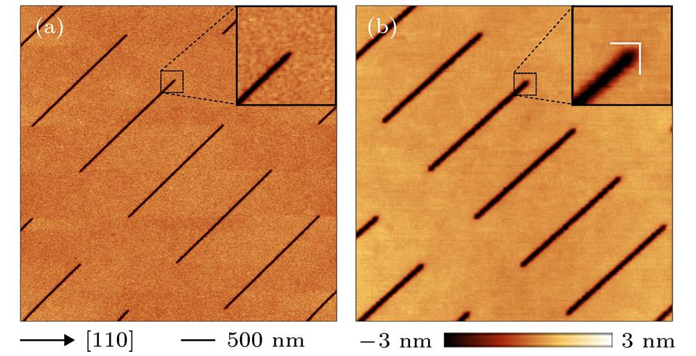
    Fig. 1. AFM image of the trench-patterned Si substrate before (a) and after (b) the growth of Si buffer layer, insets are the zoom-in images of one end of a trench before and after the Si buffer layer, respectively.生长硅缓冲层前(a)和生长硅缓冲层后(b)硅周期性凹槽结构的表面AFM图, 插图分别为生长硅缓冲层前后凹槽末端的放大图
    (a) AFM image of ordered GeSi wires on trench patterned substrate; (b) AFM image of zoom-in individual GeSi nanowire; (c) AFM linescan along the cross-section of a GeSi nanowire. Inset scale bar: 500 nm.(a)硅衬底上有序锗硅纳米线的AFM图; (b)单根锗硅纳米线的AFM图; (c)单根纳米线的表面线扫描图, 图中标尺均为500 nm
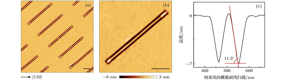
    Fig. 2. (a) AFM image of ordered GeSi wires on trench patterned substrate; (b) AFM image of zoom-in individual GeSi nanowire; (c) AFM linescan along the cross-section of a GeSi nanowire. Inset scale bar: 500 nm.(a)硅衬底上有序锗硅纳米线的AFM图; (b)单根锗硅纳米线的AFM图; (c)单根纳米线的表面线扫描图, 图中标尺均为500 nm
    AFM images of the trench-patterned samples with 4 nm Si67Ge33 film after 1 h annealing at different temperatures: (a) 450 ℃; (b) 500 ℃; (c) 510 ℃; (d) 520 ℃; (e) 530 ℃; (f) 550 ℃.在硅凹槽结构图形衬底上沉积4 nm的Si67G33薄膜, 然后在不同温度退火后得到的样品表面AFM图 (a) 450 ℃; (b) 500 ℃; (c) 510 ℃; (d) 520 ℃; (e) 530 ℃; (f) 550 ℃
    Fig. 3. AFM images of the trench-patterned samples with 4 nm Si67Ge33 film after 1 h annealing at different temperatures: (a) 450 ℃; (b) 500 ℃; (c) 510 ℃; (d) 520 ℃; (e) 530 ℃; (f) 550 ℃. 在硅凹槽结构图形衬底上沉积4 nm的Si67G33薄膜, 然后在不同温度退火后得到的样品表面AFM图 (a) 450 ℃; (b) 500 ℃; (c) 510 ℃; (d) 520 ℃; (e) 530 ℃; (f) 550 ℃
    The influence of Ge concentration on the formation of SiGe wires when the thickness of SiGe film is fixed: (a) Si68G32; (b) Si66G34; (c) Si63G37.固定薄膜厚度时, 锗的含量比例对纳米线结构的影响 (a) Si68G32; (b) Si66G34; (c) Si63G37
    Fig. 4. The influence of Ge concentration on the formation of SiGe wires when the thickness of SiGe film is fixed: (a) Si68G32; (b) Si66G34; (c) Si63G37. 固定薄膜厚度时, 锗的含量比例对纳米线结构的影响 (a) Si68G32; (b) Si66G34; (c) Si63G37
    AFM images of GeSi wires on trench-patterned Si (001) with different pattern periods: (a) period of 2 µm; (b) period of 500 nm.不同周期图形衬底上锗硅纳米线的表面AFM图 (a)周期为2 µm; (b)周期为500 nm
    Fig. 5. AFM images of GeSi wires on trench-patterned Si (001) with different pattern periods: (a) period of 2 µm; (b) period of 500 nm.不同周期图形衬底上锗硅纳米线的表面AFM图 (a)周期为2 µm; (b)周期为500 nm
    Fei Gao, Qi Feng, Ting Wang, Jian-Jun Zhang. Controllable growth of GeSi nanowires on trench patterned Si(001) substrate[J]. Acta Physica Sinica, 2020, 69(2): 028102-1
    Download Citation